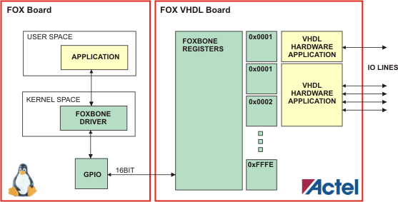
Architecture of the FOXBONE
The FOXBONE interfacing protocolwritten by Sergio Tanzilli and Roberto AsquiniFoxBone is the way to exchange data between Fox and FOXVHDL boards |
@include='123' |
A convenient and efficient way of communication between the Fox Board way of communications is needed to take advantage of this flexibility without sacrificing generality and speed. For this reason we present the FOXBONE bus architecture, a very simple and convenient protocol that permits the data exchange between Fox Board and Fox VHDL in a register oriented structure inside the FPGA. A special designed kernel driver named "foxbone" is available for userspace applications to communicate with the hardware functions registers inside the FPGA at higher speed respect to the use of the GPIO kernel driver.
It is possible to build specific kernel drivers for the hardware peripherals inside the FPGA so that application programs in userspace can use them seamlessly and very easily at max speed.
Architecture of the FOXBONE
Enabling an effective way of communication between the Fox Board and several custom logic blocks is a complex task since it has to satisfy several constraints. The architecture power and size of nowadays FPGA components lets to design and embed several different functions inside the same FPGA component that will work all in parallel, the FoxBone protocol should be flexible enough to let the Fox Board to effectively communicate to those different hardware functions with a limited number of electrical wires and to provide room for other additional ones without have to redesign the protocol. Another rule of design is to not impose policy on the protocol so to let it free for designer customization and to offer a common base leaving extension space for special needs without loss of generality.
Addressing scheme
The solution here proposed is to have an addressable 16 bit I/O (input/output) asynchronous interface to a series of 16 bits registers inside the FPGA which control the internal functions. The meaning of the registers and the number of them for every function is function specific so no assumption or policy is forced on the FoxBone bus. Through it the Fox Board will be able to read from a maximum of 65536 FPGA 16 bit registers (to be written by the FPGA) and to write to up to 65535 FPGA 16 bit different registers to be read from the programmable logic to directly control it.
To be able to reuse different functions without (if possible) rewrite the VHDL code we are suggesting a fixed addressing numbering space for every function we will present on these pages. So for example picking up the VHDL code for function1 that uses registers 3000h and 3001h and function4 that uses register from 2340h to 2347h, since both are using the Fox Bone interface they will cohexist inside the FPGA chip without problems. Also the kernel drivers will refer for every specific function to their fixed address, so it will be possible to assemble different ready built VHDL functions inside the FPGA from our library and continue to use our kernel drivers to access them from userspace programs without addressing problems. A range of 65000+ addresses should be enough (at least for these first releases of the protocol) to accommodate several different functions.
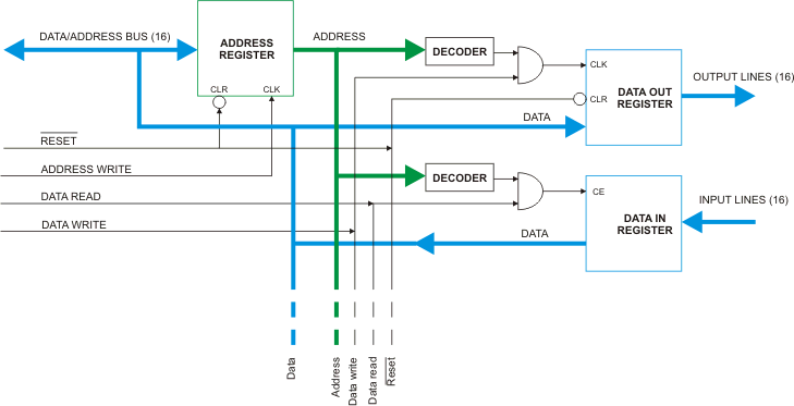
Inside the FPGA we will arrange the logic for a 16 bit address register and the decode logic for every data register needed by every function.
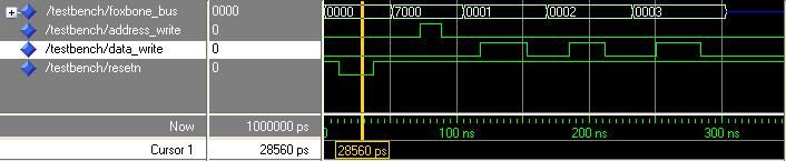
To limit the number of I/O lines the architecture of the bus (FOXBONE_BUS) is based on 16 bits for multiplexed addresses and data. So the Fox Board foxbone software will present first the desired address to be used, then it will write it in a special address register inside the FPGA. Then the Fox will read or write from/to this register preselected using the 16 I/O lines as data lines.
After loading in the first phase of the 16 bit I/O bus transaction the desired address, a line (ADDRESS_WRITE) will be used to write this required FPGA register address to be written or read, inside the FPGA address register.
Another line (DATA_WRITE: active high) will be used in the second part of the transaction from the Fox to store the data in the previously addressed register of the FPGA.
The signal (DATA_READ: active high) is used instead from the Fox to read the previously address selected register from the FPGA.
A Reset signal (RESETN: active low) can be used from the Fox Board to initialize all the FPGA hardware registers and interface logic to a defined initial state.
An interrupt line to the FOXBOARD (active high) will enable the requesting of services for data transfers to/from the FOXVHDL with a mechanism to enable multiple interrupt sources through a interrupt registers scheme readable from the Fox Board.
DATA_READ:     Og1 (Fox J6:23) (Fox output)
ADDRESS_WRITE: Og4 (Fox J6:25) (Fox output)
DATA_WRITE:    Og2 (Fox J6:21) (Fox output)
INT:           PA0 (Fox J7:38) (Fox input)
RESETN:        Og3 (Fox J6:26) (Fox output)
Starting from all the five control signals (4 output and 1 input from the Fox side) in the low logic state we are in the reset state for the FPGA. Now after raising the Reset signal we will have the FOX VHDL ready to exchange data on the FoxBone interface with the Fox Board.
Reset phase: With any value (in the present specification) on the FOXBONE_BUS lines, pulse the RESETN line down once to reset all the logic registers inside the FPGA.
Then, starting from all signals low and RESETN high, the software driver program on the Fox Board has to do the following steps to write on the FPGA register 0x8000 through the Fox Bone and read it back:
The final signal values will be all low except for the Reset signal
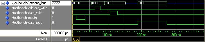
Repeat all the above steps to write or read in other registers.
We are using this mode for example to transfer video buffers to the FOX VHDL Board from the Fox. Inside the FPGA has been realized a logic that stores the value on the bus at the rising edge of the DATA_WRITE signal and increments an internal counter (used as internal buffer address) on the falling edge of the DATA_WRITE signal.