 ## Debug port
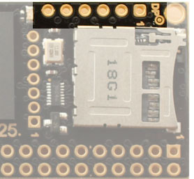
This port is designed to be used with the
* [Debug Port Interface](/DPI) or
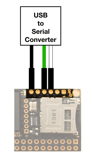
* [USB to serial converter](/USB-3V-SER)
to have access to the debug messages sent by the Atmel MPU at startup (RomBOOT),
during AT91Bootstrap second level boot loader and the Linux Kernel bootstrap.
From this port is is possible to Login directly to the Linux console
using a simple serial terminal emulator on your PC.
## Debug port
This port is designed to be used with the
* [Debug Port Interface](/DPI) or
* [USB to serial converter](/USB-3V-SER)
to have access to the debug messages sent by the Atmel MPU at startup (RomBOOT),
during AT91Bootstrap second level boot loader and the Linux Kernel bootstrap.
From this port is is possible to Login directly to the Linux console
using a simple serial terminal emulator on your PC.
|
|
| Pin # | Signal | Dir | Description | |-------|---------------|-----|-------------------------------------------------------| | DP.1 | 3V3 power out | OUT | Output from the internal regulator from 5 to 3.3 volt | | DP.2 | EN5V input | INP | If low turn off internal regulator from 5 to 3.3 volt | | DP.3 | DTXD | OUT | Debug port serial output at 115200,N,8,1 3V3 level | | DP.4 | DRXD | INP | Debug port serial input | | DP.5 | WKUP | INP | Atmel MPU wakeup signal | | DP.6 | GND | | Signal ground | |
 ## WiFi module placement
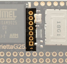
This port is designed to place this [WiFi module](/WIFI-2).
## WiFi module placement
This port is designed to place this [WiFi module](/WIFI-2).
|
| Pin # | Signal | Dir | Description | |-------|---------------|-----|-------------------------------------------------------| | 7 | WPS | OUT | WSP function. Low level activated. Wired to PC16 | | 6 | LED | N.C.| WiFi module activity led. Not used | | 5 | GND | | Signal ground GND | | 4 | USB B D+ | | USB Host B D+ | | 3 | USB B D- | | USB Host B D- | | 2 | VCC 3.3V DC | OUT | Output from the internal regulator from 5 to 3.3 volt | | 1 | WiFi TXEN | OUT | RF on/off control. Low level activated to off. Wired to PC30 | |