Arietta technical documentation Buy
Arietta pinout
This is the default pinout of Arietta G25 when you use the latest default image available in the image repository.
It is possible to change it by using the Device tree compiler and dynamic Arietta G25 pinout page

Debug port
This port is designed to be used with the
to have access to the debug messages sent by the Atmel MPU at startup (RomBOOT), during AT91Bootstrap second level boot loader and the Linux Kernel bootstrap.
From this port is is possible to Login directly to the Linux console using a simple serial terminal emulator on your PC.
|
|

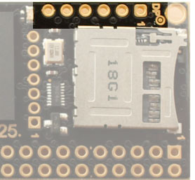
WiFi module placement
This port is designed to place this WiFi module.
To know hot to configure it: Using the WIFI module on Arietta G25

|
|
Schematic
To know more about how are routed each signal inside the Arietta board please take a look to the Arietta schematic.