FVBE - TimeBase1by Roberto AsquiniBuild a 32 bit precision timer with 15nsec of resolution |
This example presents a programmable 32 bit timer with resolution of 15.625 nsec and max period of 67 seconds. It can be used to generate very precise periodic pulses for by other peripherals or to trigger timed events or operations. The example will show how to program it to light up an external LED for a precise semiperiod of 1.0000 second and how to change the timer values through several foxbone interfaces. This example uses, as usual, a Fox Board coupled with a Fox-VHDL board.
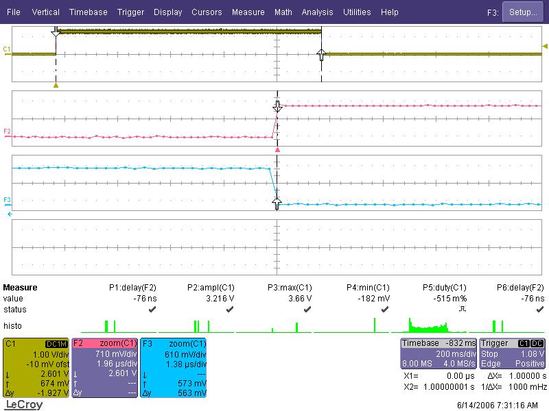
Real measure of the TimeBase1 TIMEBASEHALFOUT output signal
The above screenshot shows the oscilloscope result output of the 32 bit timer function TimeBase1. It is possible to see, in the highest green trace, the 1.00000 second semiperiod generated by the Fox-VHDL board output H13 TIMEBASEHALFOUT. In the two traces underneath there are the rising and falling fronts of the signal zoomed to show the precision of the measure.
Signature release register values for this example:
	0x0004=0x0070
	0x0005=0x2323
	0x0006=0x0001
	0x0007=0x0001
The example is composed of two VHDL files: TimeBase1.vhd that realizes the inner part of the example with the logic needed to implement the 32 bit timer-counter and the logic for resetting it at the desired value. The other file FoxBone_TimeBase1.vhd is a wrapper file that permits the working of the timer under the FoxBone specifications. So we will be able to access the timer functionalities through some foxbone registers.
In particular, these are the relevant FoxBone registers for this application and their meaning:
- -- 0x0004: readable register returning the FoxBone release (presently 0x0070 or 0.7.0)
- -- 0x0005: first hardware application word returning 0x2323 (FoxBoneExamples)
- -- 0x0006: second hardware application word returning 0x0000 (stands for example 1)
- -- 0x0007: third hardware application word returning 0x0001 (release 1 of example 1).
Those above registers are present in every foxbone implementation to help the application software to recognize the correct programmed FPGA inside the Fox-VHDL board to avoid uncorrect driving of the hardware peripherals inside the FPGA.
- -- 0x0100: read/write register with the bit 0 meaning enable for the TimeBase: 1 = enabled
Startup value = 0x0001 (enabled) - -- 0x0102: read/write register with the low 16 bit part of the time base preset value
Startup value 0x8fff. - -- 0x0103: read/write register with the high 16 bit part of the time base preset value
Startup value 0x03d0. (Both registers are preset at startup for a total delay of 1.0000 seconds).
How it works
The 32 bit timer application example uses a 32 bit counter clocked by the main external clock of the Fox-VHDL board (frequency: 64 MHz; period: 15.625 nsec). The free running counter value is compared constantly against a 32 bit (programmable through FoxBone) value named DIVIDERVALUE. When there is a match, a positive pulse of 15.625 nsec is generated on the external output TIMEBASEOUT on the FPGA pin H14 that is connected to the Fox-VHDL pin JP3.23. Moreover the matching has the effect of resetting the 32 bit counter, so that a whole time interval will be waited as programmed. The total number of clock ticks for every round of the counter will be DIVIDERVALUE +1. To take advantage of the timer output in a different way, since the generated pulse is very short in time, another output is generated with a logic divider by two feeded by the generated pulse. Its output will be half frequency square wave but with a 50% duty cycle. So, its semiperiod will equal the programmed interval timer. This signal is routed out of the FPGA on the line TIMEBASEOUTHALF on the FPGA pin H13 that corresponds to the external Fox-VHDL pin JP3.24. At this line we can connect an external LED or an oscilloscope to show the timer operation.
How to test it immediately
To try immediately the 32 bit timer function you can download and save on your PC the FPGA programming file: FoxBone_TimeBase1.stp.
Then follow the programming instructions on: Flashing the FOX VHDL FPGA with a new hardware image to program the Fox-VHDL FPGA.
To program the FPGA and test it you should have the Fox programmed with a fimage capable to drive the Fox-VHDL board.
Hardware test bench
Now we are ready to test our Fox-VHDL Example TimeBase1. As shown in the figure below, connect a normal Led to pin JP3.24 and ground (GND) through a 1000 Ohm resistor.
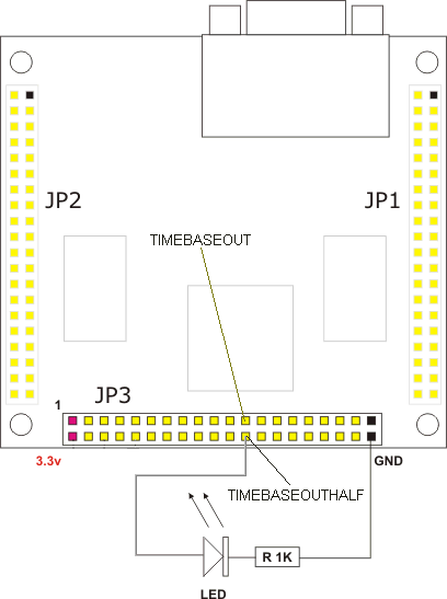
Schematic of the hardware connection
After the start of the Fox Board and the FOX VHDL you should observe the external LED just connected, cycling with on and off periods of exactly 1 sec each. To change this time period just refer to the article How To change FoxBone registers from the FOX BOARD .
Using one of the methods described in the article change the values of the registers 0x102 and 0x103. Observe consequently, the on and off variation of time semiperiods of the LED.
Beware when modifying the foxbone registers 0x102 and 0x103. if the timer is running since if you change the value with a lower value in a moment when the running 32 bit counter has just passed that value, the matching comparison will be delayed to a complete round of the 32 bit counter so you must wait up to 67 seconds to have the register change operative. It can result in an apparent freeze of the function. To avoid this, better to stop the timer before changing its register values. To stop the timer counter and reset it to zero, just write 0x0000 into the register 0x100. After the change on the registers 0x102 and 0x103 restart the timer with a write operation of 0x0001 in the 0x100 register.
Test the 32 bit timer with the timebase application
Inside the FOX image able to program and drive the FOX VHDL board, there is also installed a kernel driver specifically designed to operate with the foxbone registers of the foxbone timebase application. In other articles we will explain how to build a Linux kernel driver for a foxbone peripheral so to exploit the max performances from it. Here we would like to show a simple way to interact with the Timebase function with a simple command line tool that is also inside the FOX Board image fimage_300_v100.zip.the timebase tool
# timebase
timebase usage: timebase command value
valid commands:
e = enable timebase;
d = disable timebase;
h = set high timevalue;
l = set low timevalue

Typical usages:
timebase e (enable)
timebase h 1d0 (set high value to 0x1d0 which)
               (makes the led blink fast)
As you can see above, invoking timebase from a console or telnet session of the FOX, you can have the possible options to use the tool. You can enable or disable the timebase (so stopping the LED from blinking) or change the lower word or the higher word of the 32 bit timebase preset value. It is very simple to use this tool also inside a script. Here is reported the sourcecode of the timebase tool to show the way to write a program that uses the custom kernel driver of the timebase foxbone function: timebase.c
In Depth: TimeBase1.vhd description
The VHDL code TimeBase1.vhd implements the inner part of this example. In our examples we always detach the function application specific code files from the FoxBone interface file that is put above it in a hierarchical way. This decoupling permits a cleaner way of programming the internal hardware functions separating them from the details of the foxbone interface needed to operate it. It is a good common practice that permits an easy reuse and multiple use of the hardware function logic blocks. The wrapping VHDL code file for this example (FoxBone_TimeBase1.vhd) will be presented later on.
As you can see, at the beginning of the TimeBase1.vhd VHDL file it is declared an entity named TimeBase1 that has the following port signals:
- CLOCK that is used to connect the main clock for the working of the logic.
- TIMEBASEOUT This is one of the two outputs of this function. It goes high for 15.625 nsec every time the 32 bit counter reaches the DIVIDERVALUE value.
- RESETN This signal is used to stop and reset all the logic of this function logic block.
- DIVIDERVALUE This is a port signal that is set from outside this module and is here used as comparison value for the running counter to reset the counter when matching and to generate TIMEBASEOUT pulses.
- RUNCOUNTER This port is made available for hierarchical higher codes to have information around the actual value of the running counter.
After the declaration of two internal signals we see the presence of two processes that together realize the complete 32 bit timer function. Let's see the first process:
  RunningCounterProcess : process (RESETN, resetCounter, CLOCK)
  begin
    if ( RESETN = '0' or resetCounter = '1') then
      RunningCounter <= x"00000000";
    elsif ( CLOCK'event and CLOCK = '1') then
      RunningCounter <= RunningCounter + 1;
    end if;
  end process;
This first process is sensitive to three signals: RESETN, resetcounter
and CLOCK. This process acts on the RunningCounter 32 bit internal signal.
It resets the RunningCounter when either RESETN = '0' or the internal
signal resetCounter is at level '1';
otherwise at every CLOCK rising front the RunningCounter value
is incremented.
Let's see now the second process:
  resetCounterprocess : process (RESETN, CLOCK)
  begin
    if ( RESETN = '0' ) then
      resetCounter <= '0';
    elsif ( CLOCK'event and CLOCK = '0') then
      if (RunningCounter = DIVIDERVALUE) then
        resetCounter <= '1';
      else
        resetCounter <= '0';
      end if;
    end if;
  end process;
The second process initializes at zero the internal signal resetCounter
during RESETN = '0'. Then on every falling edge of the
CLOCK signal it is made a comparison between the DIVIDERVALUE
value and the RunningCounter value. If they are equal, the internal
signal resetCounter is set. Otherwise (no matching values) the
resetCounter signal is reset. The second process realizes a standard
32 bit logic comparator.
Making the comparison on the negative front of the CLOCK port signal is useful to avoid logic races on the increment of the RunningCounter that is incremented on the rising edges of the CLOCK.
@idea To better understand race conditions in logic design please see this article: Understanding Race Conditions in Logic Programming.
The set of the resetCounter signal will reset RunningCounter to all zeroes value so restarting the whole process.
In the last part of the code, the internal signal resetCounter is connected to the port signal TIMEBASEOUT, so it will be available outside the entity TIMEBASE1. It is the main output for this function. As well the internal runningCounter signals are connected to the port signal RUNCOUNTER so other entities outside this module can read it for their use. It offers a view of the current timebase value. The connection of the internal signals to port signals declared in the entity also permits to visualize them during simulation session.
In the following you can see a simulation diagram of the TimeBase1.vhd VHDL code. This simulation has been made using the standard tools inside the Actel suite of programs Libero 7.1:
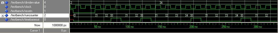
Simulation diagram of TimeBase1 VHDL code
Is it possible to see in the diagram that when the signal resetn (the simulator ignores the uppercase of the names) is at a low state the runcounter port signal that replicates the internal signal RunningCounter is fixed at zero and is not incremented by the clock port signal. After the rising front of resetn, runcounter starts counting up at every rising front of the clock.
In the highest part is it possible to see the value set for dividervalue that is 2. When the runcounter reaches the value 2, at the clock falling edge, the runcounter value shows that the runningCounter has been reset and the port signal timebaseout is set for one clock period of time. timebaseout is reset at the next clock falling edge and runcounter can then restart counting again from the next rising front of the clock port signal. This is why the total period exceed by 1 the value of the DIVIDEVALUE signal. Infact the rising fronts of the timebaseout signal are distant here three clock periods.
Changing the dividervalue to 4, will change the time period of the timebaseout pulses from 2+1 to 4+1 clock periods.
Asserting low the port signal resetn stops and resets the runcounter 32 bit counter.
In Depth: FoxBone_TimeBase1.vhd description
The VHDL code FoxBone_TimeBase1.vhd implements the outer part (or interface part) of this example.
This is the root part of the VHDL project so the relative entity port signals will all be connected to real pins of the FPGA. In the following the list of the external pins to operate this function through FOXBONE. We can see so in the entity FoxBone_TimeBase1, the declaration of the 32 bit FOXBONE_BUS and the other 4 foxbone control signals:
- ADDRESS_WRITE
- DATA_WRITE
- DATA_READ
- RESETN
The present port signal RESETN is not the same as in the previous file TimeBase1.vhd. It is a different signal. Every signal visibility is inside its architecture definition. To connect together signals between two architectures you have to use port signals in the entity/component relationship as explained in the Introduction of VHDL coding.
The other port signals declared in the main entity for this project are:
- CLOCK that is the external main clock present on board (64 MHz);
- TIMEBASEOUT is the output for the pulse generated by the timer when the counter matches the dividervalue programmed in the foxbone registers 0x102 and 0x103.
- TIMEBASEHALFOUT is instead a signal generated in this file to have a signal of 50% duty cycle that we will connect to a LED for demonstration purposes. It realizes a "use" of the 32 bit timer to generate a simple flasher with equal times for on and off.
In the architecture part of the code we see firstly a group of eight 16 bit constants that implement the constant foxbone register addresses and values. The following constants represent the addresses chosen for the specific registers of the TimeBase1 function:
- TIMEBASE_ENABLE_CONTROL_REGISTER_ADDRESS: address 0x100. Bit 0 of this register is to enable/disable the 32 bit timer.
- TIMEBASE_LOW_VALUE_CONTROL_REGISTER_ADDRESS: low word timer value (will be passed to the low part of DIVIDERVALUE of TimeBase1).
- TIMEBASE_HIGH_VALUE_CONTROL_REGISTER_ADDRESS: high word timer value (will be passed to the high part of DIVIDERVALUE of TimeBase1).
Now we found the declaration of the component TimeBase1. This is the standard way to decompose a logic task in a hierarchical way with several files. The component will be instantiated later and the port signals of the component will be connected to the respective port signals of the entity TimeBase1. so they must have always a perfect correspondence in terms of bit width and meaning to couple together.
Then we see the definition of the internal signals.
The simple declaration of a signal (single bit or multibit) is enough to realize a permanent register inside the FPGA that can be written or read inside the scope of the signal itself that is inside the architecture where the signal has been declared.
The Address signal realizes the FoxBone Address Register; TimeBaseLow and TimeBaseHigh are the place to store the 32 bit DIVIDERVALUE that is the preset value for the timer. They will be joined to form a single 32 bit value in TimeBaseValue. The signal TimeBaseEnable is the register to enable or disable (with its bit 0) the Timer. Then there is the declaration of TimeBaseOutput and TimeBaseHalf50Duty that will bring the resulting outputs to the port signal for external access. The last signal declared dummyRunCounter is not stricly necessary if we don't need to have the TimeBase1 running counter value available outside the FPGA chip (or for simulation purposes).
Ended the signal declaration part of the code, we start with the interconnection part between signals and direct asynchronous statements with the desired combination of logic operations needed:
  -- this is the address register
  Address <= (others => '0') when RESETN = '0' else
             FOXBONE_BUS when ADDRESS_WRITE = '1';
The above statement realizes the working of the FoxBone Address register. The Address internal 16 bit signal is assigned a '0' value when the external RESETN signal is at low logic state. Otherwise it is asynchronously assigned the value present on the FOXBONE_BUS if the external port ADDRESS_WRITE is at high logic state (this follows the FoxBone 0.7.0 specifications). This statement will be implemented inside the FPGA with combnatorial logic so it will be always working asynchronously with respect to other statements and processes inside the FPGA.
Now is the part realizing the addressing for the internal constant release registers:
  -- input from release registers
  FOXBONE_BUS <= RELEASE_REGISTER_0_VALUE when Address = RELEASE_REGISTER_0_ADDRESS
                 and DATA_READ = '1' else  (others=>'Z');
  FOXBONE_BUS <= RELEASE_REGISTER_1_VALUE when Address = RELEASE_REGISTER_1_ADDRESS
                 and DATA_READ = '1' else (others=>'Z');
  FOXBONE_BUS <= RELEASE_REGISTER_2_VALUE when Address = RELEASE_REGISTER_2_ADDRESS
                 and DATA_READ = '1' else (others=>'Z');
  FOXBONE_BUS <= RELEASE_REGISTER_3_VALUE when Address = RELEASE_REGISTER_3_ADDRESS
                 and DATA_READ = '1' else (others=>'Z');
This statements put on the FOXBONE_BUS the value of the addressed release register written on the Address internal signal register when the external port signal DATA_READ is at low logic state. Otherwise the FOXBONE_BUS is released to let other uses of the bus.
This is a simple (however not the best in logic occupation efficiency) way to make the decode of the Address value for the read of a register. In this way every register takes care of its logic decoding and it is very simple to add new registers or to cut them without affecting the remaining ones compared to a solution with a decode module that decodes all the addresses for all the registers, that would be more efficient in terms of logic gate occupation but monolithic and more difficult to extend for new registers and functions.
Now we have the function specific foxbone register read/write part:
  -- write operation to the TimeBase Enable Register to set its value
  TimeBaseEnable <= x"0001" when RESETN = '0' else
                    FOXBONE_BUS when Address = TIMEBASE_ENABLE_CONTROL_REGISTER_ADDRESS
and DATA_WRITE = '1';

  -- write operation to the TimeBase Low Value Register to set its value
  TimeBaseLow <= x"8fff" when RESETN = '0' else
                 FOXBONE_BUS when Address = TIMEBASE_LOW_VALUE_CONTROL_REGISTER_ADDRESS
and DATA_WRITE = '1';

  -- write operation to the TimeBase High Value Register to set its value
  TimeBaseHigh <= x"03d0" when RESETN = '0' else
                  FOXBONE_BUS when Address = TIMEBASE_HIGH_VALUE_CONTROL_REGISTER_ADDRESS
and DATA_WRITE = '1';

  -- read from the TimeBase Enable Register to read its value
  FOXBONE_BUS <= TimeBaseEnable when Address = TIMEBASE_ENABLE_CONTROL_REGISTER_ADDRESS
and DATA_READ = '1' else (others=>'Z');
  -- read from the TimeBase Low Value Register to read its value
  FOXBONE_BUS <= TimeBaseLow when Address = TIMEBASE_LOW_VALUE_CONTROL_REGISTER_ADDRESS
and DATA_READ = '1' else (others=>'Z');
  -- read from the TimeBase High Value Register to read its value
  FOXBONE_BUS <= TimeBaseHigh when Address = TIMEBASE_HIGH_VALUE_CONTROL_REGISTER_ADDRESS
and DATA_READ = '1' else (others=>'Z');
We can see the VHDL code to act on the internal signals relative to the TimeBase registers. TimeBaseEnable is preset at 0x0001 (Timer enabled) at startup (when RESETN = '0') otherwise will be written by the FOXBONE_BUS when it is made a write operation on its address (specified above in the constant part. Similarly for the TimeBaseHigh and TimeBaseLow. Then we have the part that permits to read back those three registers that is the same we have seen for the constant release registers, using the internal signals as source to charge the FOXBONE_BUS instead of the constant values.
There is now the build of the stopTimeBase internal signal as the immediate AND operation of the RESETN external port signal and the bit 0 of the TimeBaseEnable register. stopTimeBase will be used to pass the reset command to the TIMEBASE1 component so that the internal counter will be reset and stopped either when the external FOXBONE interface is reset or when the bit 0 of the foxbone register TimeBaseEnable is at zero value. Then the two foxbone registers TimeBaseLow and TimeBaseHigh are joined together with as asynchronous statement to form the function needed 32 bit value TimeBaseValue for the DIVIDERVALUE port signal of TimeBase1.
  -- the TimeBase will be stopped (stopTimeBase<='0') when either RESETN or
  --  bit 0 of TimeBaseEnable are at '0' value.
  stopTimeBase <= RESETN and TimeBaseEnable(0);
  -- we are operating with negative logic so we need 'and' here!!

  -- here is the join of the two 16 bit TimeBase values to form
  -- the complete 32 bit TimeBase signal value
  TimeBaseValue <= TimeBaseHigh & TimeBaselow;
Now we have the real instantiation (there can be more than one instantiation of the same component in case you need more than one for your application) of the TimeBase1 component with the coupling between the component port signals and the internal signals of the present file:
  -- this is the instantiation of the TimeBase component.
  myTimeBase : TimeBase1
  port map (
    CLOCK => CLOCK,                -- input clock 64 MHz.
    TIMEBASEOUT => TimeBaseOutput, -- out timebase signal.
    RESETN => stopTimeBase,        -- reset signal (active low)
    DIVIDERVALUE => TimeBaseValue, -- 32 bit divider value
    RUNCOUNTER => dummyRunCounter
  );
We see that the external CLOCK is passed directly to the component TimeBase1. Also the mapping for the other signals is to pass inside the component the right signals and to extract the output signals to be used outside it.
Finally we have a simple process that uses the main output port signal of the TimeBase1 component TIMEBASEOUT, mapped to TimeBaseOutput to generate a 50 % duty cycle signal with half the frequency of TimeBaseOutput:
  -- this process takes the output of the TimeBase and
  -- divide it by two obtaining a 50 % duty cycle signal
  -- with half the frequency of the original TimeBase signal.
  timebaseDividerProcess : process (stopTimeBase, CLOCK, TimeBaseOutput)
  begin
    if ( stopTimeBase = '0' ) then
      TimeBaseHalf50Duty <= '0';  -- initialization
    elsif ( CLOCK'event and CLOCK = '1') then
      if (TimeBaseOutput = '1') then
        TimeBaseHalf50Duty <= not TimeBaseHalf50Duty;
      end if;
    end if;
  end process;
This above process will produce the internal signal TimeBaseHalf50%Duty. This process is sensitive to three signals:
- stopTimeBase: above generated;
- CLOCK: main clock;
- TimeBaseOutput: the main output from the TimeBase1 component
The last two statements only map the two internal signals constituting the real outputs fo this application to two port signals for this entity (that is the root file of the project), making them available outside the FPGA when mapped to a specific pin during the physical constraints Designer phase of the Libero compilation of the code.
Simulation of the FoxBone_TimeBase1.vhd project
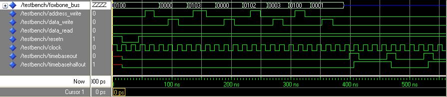
Simulation diagram of FoxBone_TimeBase1 VHDL code
It is possible to see in the above diagram, realized with the ModelSim simulator inside the Actel Libero suite, the complete simulation of the timer operation inside the foxbone architecture.
Firstly we have the reset stage of the foxbone interface, then the write on the register 0x100 of the '0' value, stopping the timer operations. Then we see the write on the registers 0x103 (high part) and 0x102 (low part) of the combined value 0x00000003 (we use low values to have a comprehensible view in the simulation). After setting the internal registers 0x102 and 0x103 for the DIVIDERVALUE, we release the timer counter writing a '1' on the 0x100 register. Just after the release of the timer we see activity on the timebaseout port signal that goes high at every 3+1 clock pulses (see the working of TimeBase1.vhd to see why).
Finally, the port signal timebaseouthalf will generate the supposed signal with half the frequency of timebaseout and 50% duty cycle. We used this signal to connect to the external LED for visualization after putting the registers 0x102 and 0x103 at a value such as to generate precise 1.000 second semiperiods of the timebaseouthalf port signal.
Libero Designer Layout Report
This is the Status Report that can be obtained in the Libero Designer session under the Menu: Tools - Reports - Status Report after the Layout compiling phase of the project.
Compile report:
===============

    CORE                     Used:    356  Total:   6144   (5.79%)
    IO (W/ clocks)           Used:     23  Total:    157   (14.65%)
    Differential IO          Used:      0  Total:     38   (0.00%)
    GLOBAL (Chip+Quadrant)   Used:      1  Total:     18   (5.56%)
    PLL                      Used:      0  Total:      1   (0.00%)
    RAM/FIFO                 Used:      0  Total:      8   (0.00%)
    FlashROM                 Used:      0  Total:      1   (0.00%)
As you can see the 32 bit timer function and all the FoxBone interface and registers are occupying only 5.79% of the FPGA logic space.
Download the whole project to install and recompile it in your PC
Here is the link to download a zipped copy of the entire FoxBone_TimeBase1.zip Libero 7.1 project. Please refer to the Libero projects download and installation page to be able to recompile the project, to simulate it and generate the programming .stp file to program the Fox-VHDL FPGA.The only very important file to consider other than the .vhd files of the project, is the physical constraint file that maps the port signals of the VHDL project to the physical pins of the FPGA. It is easy to see that the maximum effort has to be applied to avoid mistakes on this file, since a wrong map of an output of the Fox_VHDL board to an output of the Fox Board can result in a misfunctioning or to a damage for the internal output stages of the Fox-Board or the FOXVHDL board. We provided current limitation resistors on all the lines to avoid this but we cannot guarantee against a very wrong mapping of several outputs together, so be very careful when mapping the physical pins of your application.
You can find here the FoxBone_TimeBase1.pdc constraint file that is also, when installed the project in your PC, under the projects FoxBone_TimeBase1\constraint directory. You can see in the .pdc file, for every function pin, other than the settings for its electrical behaviour, the mapping to the correct physical FPGA pin. You can face this information with the schematic file of the FOXVHDL board to see that they couple exactly for the interfacing with the Fox Board J6 and J7 connectors. The output function signals have instead been routed to the FPGA pins that are connected to the external connector JP3 of the FOXVHDL Board.
The physical constraint file is generated automatically as an export file inside the Designer session of your project. It is possible to assign the mapping of the pins in the IO Attribute Editor inside the Designer application of the Libero suite.
