FVBE - 16 Channel Pulse Width Modulator1by Roberto AsquiniBuild a 16 channel 16 bit PWM generator@update Improved release 2.0. It solves the glitch on PWM out when stop value = 0 and corrected behaviour when stop value = 0xffff. Now the PWMprocess is completely synchronous with the main clock. Files inside the article and FoxBone_PWM1.zip have been updated. |
This example presents a FoxBone programmable 16 channel 16 bit pulse width modulation hardware function with resolution for the duty cycle of 15.625 nsec and period of 1.024 msec. Every channel can be set independently using separate foxbone registers. The example will show how to use it through the foxbone register interfaces and with the pwm application on the Fox Board.
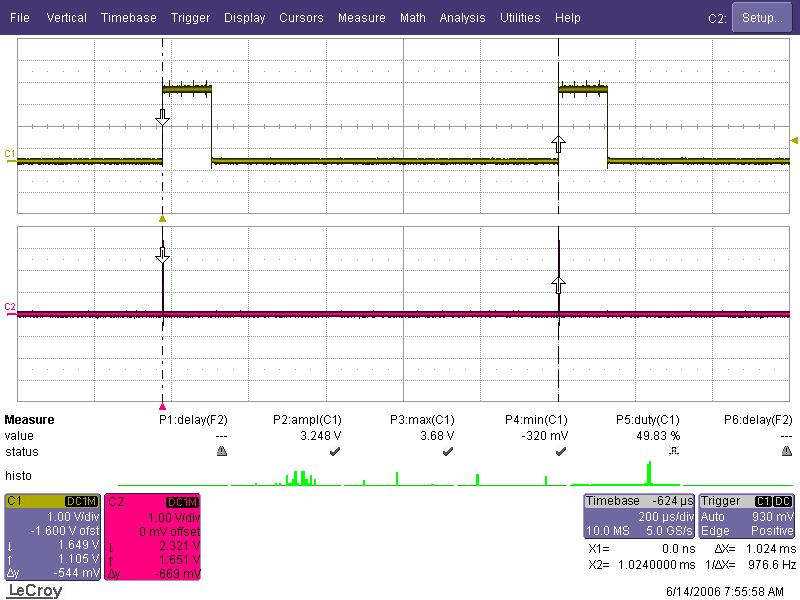
Real measure of the PWM channel 0 and its timebase signal
The above screenshot shows the oscilloscope result output of one of the 16 channels PWM and of its start period pulse (bottom trace). From the cursor readings it is possible to see the measure of the period of the start signal that is precisely 1.024 msec.
Signature release register values for this example:
	0x0004=0x0070
	0x0005=0x2323
	0x0006=0x0003
	0x0007=0x0002
The example is composed of two VHDL files: PWMchannel.vhd that realizes the inner part of the example with the logic needed to implement a single PWM channel excluding the timebase, common for all 16 channels. The other file FoxBone_PWM1.vhd is a wrapper file that uses the first VHDL code to instantiate 16 channels of PWM and generating the common 1.024 msec period start signal for all 16 channels. The change of the period PWM registers are under the FoxBone specifications. So we will be able to access the PWM functionalities through some foxbone registers.
In particular, these are the relevant FoxBone registers for this application and their meaning:
- -- 0x0004: readable register returning the FoxBone release (presently 0x0070 or 0.7.0)
- -- 0x0005: first hardware application word returning 0x2323 (FoxBoneExamples)
- -- 0x0006: second hardware application word returning 0x0003 (stands for example 3)
- -- 0x0007: third hardware application word returning 0x0001 (release 1 of example 3).
Those above registers are present in every foxbone implementation to help the application software to recognize the correct programmed FPGA inside the Fox-VHDL board to avoid uncorrect driving of the hardware peripherals inside the FPGA.
- -- 0x0050 - 0x005F: PWM channel 0 - 15 period value write only registers
Startup values:- channel0 (reg.0x0050) = 0x0800
- channel1 (reg.0x0051) = 0x1000
- channel2 (reg.0x0052) = 0x2000
- channel3 (reg.0x0053) = 0x3000
- channel4 (reg.0x0054) = 0x4000
- channel5 (reg.0x0055) = 0x5000
- channel6 (reg.0x0056) = 0x6000
- channel7 (reg.0x0057) = 0x7000
- channel8 (reg.0x0058) = 0x8000
- channel9 (reg.0x0059) = 0x9000
- channel10 (reg.0x005A) = 0xA000
- channel11 (reg.0x005B) = 0xB000
- channel12 (reg.0x005C) = 0xC000
- channel13 (reg.0x005D) = 0xD000
- channel14 (reg.0x005E) = 0xE000
- channel15 (reg.0x005F) = 0xF000
- -- 0x0060: read/write register with the enable bit for each PWM channel (0=disable; 1=enable)
Startup value 0xFFFF (all enabled).
How it works
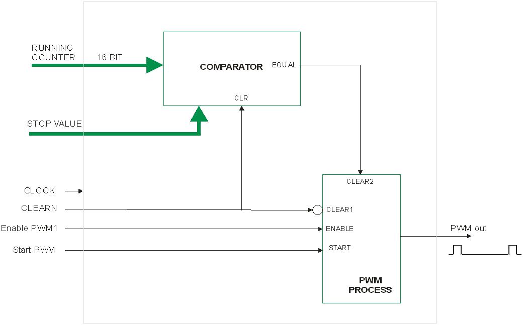
Block Diagram of a single PWM channel
There is a common 16 bit RUNNING COUNTER (RunningCounterProcess) for all the 16 PWM channels. This running counter is clocked by the master clock of the FOXVHDL board (64 MHz) so its period is 15.625 nsec.
The signal StartPWM is a pulse that goes high whenever the RUNNING COUNTER reaches the 0 count value. It is made with a logic 16 bit comparator in startPWMprocess.
STOP VAUE is a 16 bit value coming from the stop value register for the channel (writable from foxbone).
The COMPARATOR block raises its EQUAL output whenever the RUNNING COUNTER reaches the STOP VALUE count. This comparator acts on falling edges to avoid races due to the RUNNING COUNTER .
@idea To better understand race conditions in logic design please see this article: Understanding Race Conditions in Logic Programming.
The heart of the PWM generation is in the very simple PWMprocess: when EnablePWM is high the PWMout is bring at high logic state when the signal StartPWM raises (beginning of the PWM general period when RUNNING COUNTER equals zero). The EQUAL signal (RunningEqualStop) coming from the comparator then make the PWMout to fall. So changing the time when the EQUAL signal raises will change the duty cycle of the PWMout signal. This can be accomplished changing the STOP VALUE register through the foxbone interface. When EnablePWM stays low no signal is generated on PWMout.
In the main file FoxBone_PWM1.vhd there is the logic to be able to write the 16 channels Stop value registers, to read/write the EnablePWM register where each bit corresponds to a single channel enable bit and there is the instantiation of 16 PWM channels based on the PWMchannel.vhd code but connecting correctly all their bit interfaces.
How to test it immediately
To try immediately the 16 channels PWM generator you can download and save on your PC the FPGA programming file: FoxBone_PWM1.stp.
Then follow the programming instructions on: Flashing the FOX VHDL FPGA with a new hardware image to program the Fox-VHDL FPGA.
To program the FPGA and test it you should have the Fox programmed with a fimage capable to drive the Fox-VHDL board.
Hardware test bench
Now we are ready to test our Fox-VHDL Example PWM1. As shown in the list below, the 16 channels PWMout are coming out from the following JP3 output pins of the FOXVHDL connector (are shown also power pins on JP3 connector):
 JP3 pin  FPGA pin    PWM output
      1      ---        +3.3V
      2      ---        +3.3V
      6      N15      PWMOUT 0
      7      M15      PWMOUT 1
      8      M14      PWMOUT 2
      9      L16      PWMOUT 3
      10     L15      PWMOUT 4
      11     L14      PWMOUT 5
      12     ---   	+5V
      13     L13      PWMOUT 6
      14     K16      PWMOUT 7
      15     K15      PWMOUT 8
      16     K14      PWMOUT 9
      17     K13      PWMOUT 10
      18     J16      PWMOUT 11
      19     J14      PWMOUT 12
      20     J13      PWMOUT 13
      21     J12      PWMOUT 14
      22     B15      PWMOUT 15
      39     ---	GND
      40     ---	GND
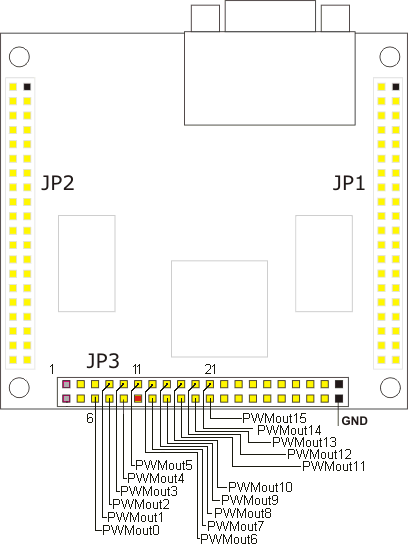
Output pins of the 16 PWM channels
You can connect LEDS between each channel and ground with a 1Kohm series resistor to see the effect of the duty cycle variation. Or, to a more precide measurement you can use an oscilloscope.
After the start of the Fox Board and the FOX VHDL you should observe the external LEDs connected connected, cycling with increasing duty cycle from 3% to 94% in relation to the value of each channel STOP VALUE REGISTER. To change these registers just refer to the article How To change FoxBone registers from the FOX BOARD .
Using one of the methods described in the article change the values of the registers 0x0050 through 0x005F. Observe consequently, the change in the duty cycle on the channel involved. To switch off one or more channel put the correspondent bit in the register 0x0060 at zero value.
@idea When modifying the foxbone registers 0x0050 to 0x005F you can obsorve a momentary high flash of the LED involved. This is because you could have changed the register value with a lower value respect to the stored one just before the Running Counter was reaching the old value. In this case there will be no match for the channels comparator so the duty cycle (just for one period) will be 100% and you will observe the high pulse flash. To avoid this effect you should modify the code adding a double buffer register so that the change in value fro every register happens only at the roundabout of the Running Counter when it reaches the zero value.
Test the 16 channel PWM with the pwm application
Inside the FOX image able to program and drive the FOX VHDL board there is also installed a kernel driver specifically designed to operate with the foxbone registers of the foxbone PWM application. In other articles we will explain how to build a Linux kernel driver for a foxbone peripheral so to exploit the max performances from it. Here we would like to show a simple way to interact with the PWM function with a simple command line tool that is also inside the FOX Board image fimage_300_v100.zip.the pwm tool
# pwm
pwm usage: foxbone command channel value
valid commands:
e = enable (value = 0 (off) or 1 (on));
p = set pwm (value = pwm frequency);
l = lights demo

Typical usages:
pwm e 1 1 (enable pwm channel 1)
pwm p 1 8000 (set frequency of channel 1 to 0x8000
#
As you can see above, invoking pwm from a console or telnet session of the FOX, you can have the possible options to use the pwm tool. You can enable or disable each channel separately or change the STOP VALUE REGISTER for each channel. It is very simple to use this tool also inside a script. Here is reported the sourcecode of the timebase tool to show the way to write a program that uses the custom kernel driver of the pwm foxbone function: pwm.c
Libero Designer Layout Report
This is the Status Report for the 16 channels PWM through FoxBone that can be obtained in the Libero Designer session under the Menu: Tools - Reports - Status Report after the Layout compiling phase of the project.
Compile report:
===============

    CORE                     Used:    869  Total:   6144   (14.14%)
    IO (W/ clocks)           Used:     37  Total:    157   (23.57%)
    Differential IO          Used:      0  Total:     38   (0.00%)
    GLOBAL (Chip+Quadrant)   Used:      1  Total:     18   (5.56%)
    PLL                      Used:      0  Total:      1   (0.00%)
    RAM/FIFO                 Used:      0  Total:      8   (0.00%)
    FlashROM                 Used:      0  Total:      1   (0.00%)
As you can see all the 16 channels of PWM and FoxBone registers are occupying only 14.14% of the FPGA logic space.
Download the whole project to install and recompile it in your PC
Here is the link to download a zipped copy of the entire FoxBone_PWM1.zip Libero 7.1 project. Please refer to the Libero projects download and installation page to be able to recompile the project, to simulate it and generate the programming .stp file to program the Fox-VHDL FPGA.The only very important file to consider other than the .vhd files of the project, is the physical constraint file that maps the port signals of the VHDL project to the physical pins of the FPGA. It is easy to see that the maximum effort has to be applied to avoid mistakes on this file, since a worng map of an output of the Fox_VHDL board to an output of the Fox-Board can result in a misfunctioning or to break the internal output stages of the Fox-Board or the Fox-VHDL board. We provided current limitation resistors on all the lines to avoid this but we cannot guarantee against a very wrong mapping of several outputs together, so be very careful when mapping the physical pins of your application.
You can find here the FoxBone_PWM1.pdc constraint file or, when installed the project in your PC, under the projects FoxBone_PWM1\constraint directory. You can see in the .pdc file, for every function pin, other than the settings for its electrical behaviour, the mapping to the correct physical FPGA pin. You can face this information with the schematic file of the Fox-VHDL board to see that they couple exactly for the interfacing with the Fox-Board J6 and J7 connectors. The output function signals have instead been routed to the FPGA pins that are connected to the external connector JP3 of the Fox-VHDL Board.
The physical constraint file is generated automatically as an export file inside the Designer session of your project. It is possible to assign the mapping of the pins in the IO Attribute Editor inside the Designer application of the Libero suite.
