FVBE - Getting startedwritten by Roberto Asquini and Sergio TanzilliA step by step guide to learn how to write VHDL applications on Actel FPGA and how to integrate them with the Linux embedded FOX Board system |
- FOX VHDL Dev Kit
@h4='120' - Actel Libero IDE Gold edition for Windows 2000/XP
Libero IDE is the most comprehensive and powerful FPGA design and development software is available, providing start-to-finish design flow guidance and support for novices and experienced users alike. Libero IDE combines Actel tools with such EDA powerhouses as Synplify, ModelSim, ViewDraw and WaveFormer Lite (tm).
This is not a tutorial about VHDL or FPGA but by reading these pages it is possible to learn something about both of them.
What is VHDL ?
VHDL is the short form of VHSIC Hardware Description Language. VHSIC is the short form of Very High Speed Integrated Circuit. (see the wikipedia definition) which means that with VHDL you can design your own application specific integrated circuit.The Actel Libero IDE Gold edition is a software suite that can compile (synthesize) your VHDL source and test (simulate) the functionality of your new hardware function.
What is a FPGA ?

|
FPGA is the short form of Field Programmable Gate Array (see the wikipedia definition) and is the chip that contains the programmable logic components and programmable interconnects used to implement physically your VHDL project.
On the FOX VHDL Board we use an Actel FPGA that has a flash memory to store our chip design that can be programmed several times directly from the FOX Board without any additional programmer using a web interface or a simple command line tool. |

|
First example: A NOT port
As a first example to see VHDL in action, we have chosen the simplest logical device: a NOT port. Let us see how to define it in VHDL, how to synthesize and transfer the hardware programming file to the FPGA memory on the FOX VHDL Board to test it.The logical schematic of a NOT port is shown below:
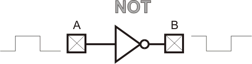
A is an input line and B is an output line. When we put on A a logic low (0 volt) B goes up to logic high (3.3 volt), when A is high B goes down.
This is the VHDL decription of a NOT port is:
library ieee;
use ieee.std_logic_1164.all;

entity VHDLNot is
    port(
         A : in std_logic;
         B : out std_logic
    );
end VHDLNot;


architecture Dataflow of VHDLNot is

begin

   B <= not A;


end Dataflow;
Follow these steps to implement your NOT chip on the FPGA:
- Download and install Actel Libero IDE Gold edition for Windows 2000/XP
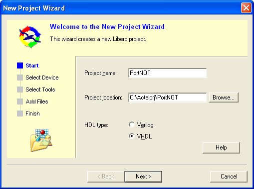
- Run it and create a new project named PortNOT from File --> New project
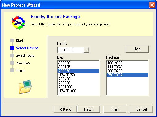
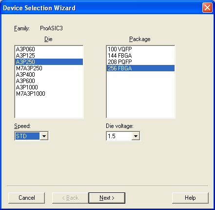
- Type Next and select Family, die and package:
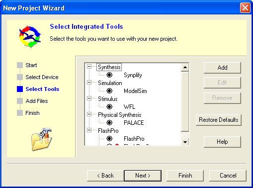
- Confirm the default integrated tools:
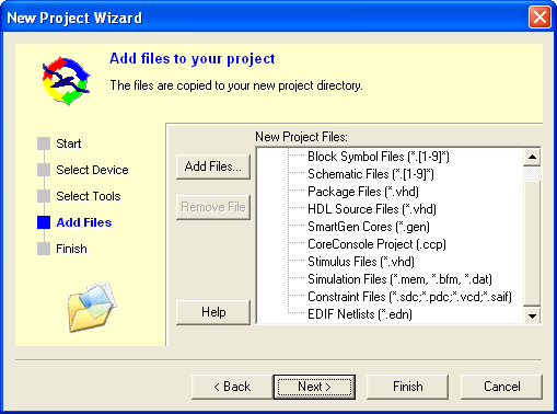
- Leave the default project files:
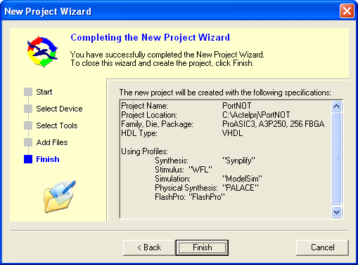
- and close the project wizard:
- Now click on HDL Editor

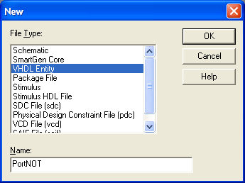
- and insert a name for your VHDL file:
- select and copy this VHDL example of code:
library ieee;
use ieee.std_logic_1164.all;

entity VHDLNot is
    port(
         A : in std_logic;
         B : out std_logic
    );
end VHDLNot;


architecture Dataflow of VHDLNot is

begin

   B <= not A;

end Dataflow;
- and paste it in the VHDL editor:
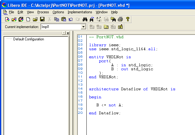
- Click on this icon to save the VHDL source file:

- Click on Design Flow tab:
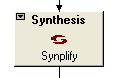
- and click on Synthesis icon to stard the VHDL source code synthesis:
- Synplify will start. Type RUN button to start the synthesis.
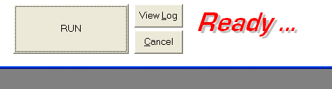
- After a while the synthesis will finish. Close the Synplify window and click
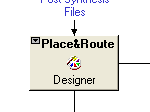
on the Place&Route icon to assign the physical pins to your NOT port.
- Designer will start. Select family, package and speed:
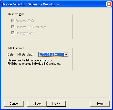
- Select the default I/O standard to: LVCMOS 3.3V:
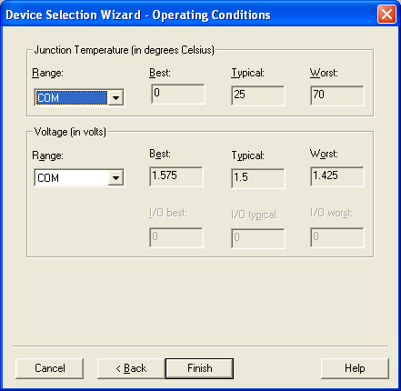
- Leave the standard operating conditions and finish.
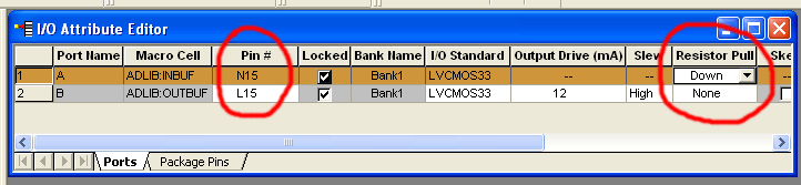
- Now you are ready to select which physically pins to use for line A and B of your NOT port. Click on I/O Attribute Editor icon:

- In the I/O Attribute Editor window assign the physical pin N15 to the A line and L15 to the B line as shown below. Assign also a pull down resistor to the input A line:
- Now commit the assignement with File --> Commit command from the window menu.
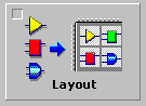
- Close the MultiView Navigator window and click on the Layout icon:
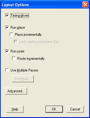
- Leave all the layout options at their default values:
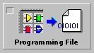
- Now click Programming File icon:
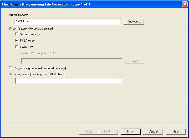
- Select the result programming file (i.e. PortNOT.stp) and Finish:
- After a while you obtain a binary with the flash image to transfer inside the FPGA. By default the file is located on the directory C:\Actelprj\PortNOT\designer\impl1.
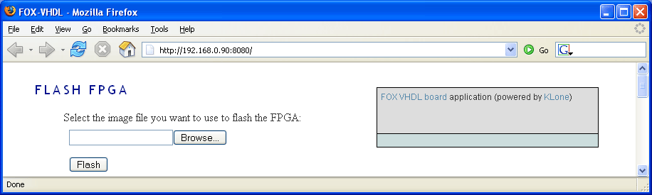
- Now start your web browser and go to the FOX Board URL:
http://192.168.0.90:8080
- then browse the hardware file PortNOT.stp and click on Flash button.
Hardware test bench
Now we are ready to test our NOT port. As shown in the figure below we can use a normal switch to set the input port (line A) and a LED to see the output state on line B.
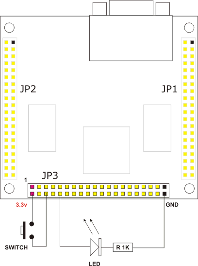
Schematic of the hardware test bench
