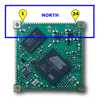
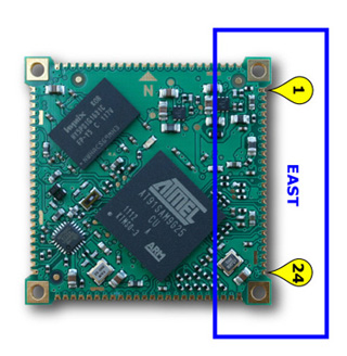
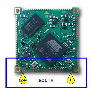
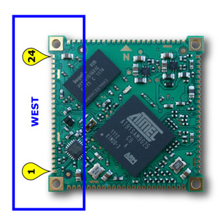
Aria technical documentation Buy

Aria G25 pinout

  • Pin # AriaG25 pin name
  • IC Pin Atmel pin name
  • Primary Line functions assigned by default at reset
  • Alt Alternative function that can be set changing the device tree binding
  • ID 2.6.x Kernel 2.6.x ID using sysfs gpio interface
  • ID 3.11.x Kernel 3.11.x ID using sysfs gpio interface
  • Note Any notes about the pin
  • Reset state Line state at CPU reset
    • PIO indicates whether the PIO Line resets in I/O mode
    • A indicates whether the peripheral A mode
    • I/O Indicates whether the signal is input or output state.
    • PU/PD Indicates whether Pull-Up, Pull-Down or nothing is enabled.
    • ST Indicates if Schmitt Trigger is enabled.

The PIO lines called PAx, PBx and PCx can be configured in up to four different ways. Please refer to the ATSAM9G25 datasheet to have a complete reference.

Be careful to check whether the line reset state is compatible with your application board because it is changed to the Linux default config during the bootstrap after at least 500 ms.

Be also careful to not leave tracks or vias not covered by solder under the Aria board, since there are testing pads on the Aria bottom.

Pin # IC Pin Primary Alt ID 2.6x ID 3.1x Note Reset state
N1 3V3 Power In Vcc
N2 PC0 GPIO SDA1 96 64 I2C bus 1 Data or GPIO PIO,I,PU,ST
N3 PC1 GPIO SCL1 97 65 I2C bus 1 Clock or GPIO PIO,I,PU,ST
N4 PC2 GPIO TIOA3 98 66 GPIO or TC block PWM0 PIO,I,PU,ST
N5 PC3 GPIO TIOB3 99 67 GPIO or TC block PWM1 PIO,I,PU,ST
N6 PC4 GPIO 100 68 PIO,I,PU,ST
N7 PC5 GPIO TIOA4 101 69 GPIO or TC block PWM2 PIO,I,PU,ST
N8 PC6 GPIO TIOB4 102 70 GPIO or TC block PWM3 PIO,I,PU,ST
N9 PC7 GPIO 103 71 PIO,I,PU,ST
N10 PC8 GPIO UTXD0 104 72 PIO,I,PU,ST
N11 PC9 GPIO URXD0 105 73 PIO,I,PU,ST
N12 PC10 GPIO 106 74 PIO,I,PU,ST
N13 PC11 GPIO 107 75 PIO,I,PU,ST
N14 PC12 GPIO TIOA5 108 76 GPIO or TC block PWM4 PIO,I,PU,ST
N15 PC13 GPIO TIOB5 109 77 GPIO or TC block PWM5 PIO,I,PU,ST
N16 PC14 GPIO 110 78 PIO,I,PU,ST
N17 PC15 GPIO 111 79 PIO,I,PU,ST
N18 PC16 GPIO UTXD1 112 80 PIO,I,PU,ST
N19 PC17 GPIO URXD1 113 81 PIO,I,PU,ST
N20 PC18 GPIO PWM0 114 82 GPIO or Pulse Width Modulation Out 0 PIO,I,PU,ST
N21 PC19 GPIO PWM1 115 83 GPIO or Pulse Width Modulation Out 1 PIO,I,PU,ST
N22 PC20 GPIO PWM2 116 84 GPIO or Pulse Width Modulation Out 2 PIO,I,PU,ST
N23 PC21 GPIO PWM3 117 85 GPIO or Pulse Width Modulation Out 3 PIO,I,PU,ST
N24 GND Power In GND


Pin # IC Pin Primary Alt ID 2.6x ID 3.1x Note Reset state
E1 GND Power In GND
E2 PC22 TXD3 GPIO 118 86 Serial line /dev/ttyS4 TXD or GPIO PIO,I,PU,ST
E3 PC23 RXD3 GPIO 119 87 Serial line /dev/ttyS4 RXD or GPIO PIO,I,PU,ST
E4 PC24 RTS3 GPIO 120 88 Serial line /dev/ttyS4 RTS or GPIO PIO,I,PU,ST
E5 PC25 CTS3 GPIO 121 89 Serial line /dev/ttyS4 CTS or GPIO PIO,I,PU,ST
E6 PC26 GPIO 122 90 PIO,I,PU,ST
E7 PC27 RTS1 GPIO 123 91 Serial line /dev/ttyS2 RTS or GPIO PIO,I,PU,ST
E8 PC28 CTS1 GPIO 124 92 Serial line /dev/ttyS2 CTS or GPIO PIO,I,PU,ST
E9 PC29 GPIO 125 93 PIO,I,PU,ST
E10 PC30 GPIO 126 94 PIO,I,PU,ST
E11 PC31 GPIO 127 95 PIO,I,PU,ST
E12 USBCP D+ USB 2.0 Host full-speed port C
E13 USBCN D- USB 2.0 Host full-speed port C
E14 GND Power In GND
E15 USBBN D- USB 2.0 Host hi-speed port B
E16 USBBP D+ USB 2.0 Host hi-speed port B
E17 GND Power In GND
E18 USBAN D- USB 2.0 Host/Device hi-speed port A
E19 USBAP D+ USB 2.0 Host/Device hi-speed port A
E20 VBAT RTC battery backup +3 volt DC input
E21 NRST Reset input signal (active low)
E22 SHDN Shutdown output signal (active low)
E23 WKUP Wake-up input signal (active low)
E24 3V3 Power In Vcc


Pin # IC Pin Primary Peripheral A ID 2.6x ID 3.1x Note Reset state
S1 3V3 Power In Vcc
S2 PA21 1W GPIO 53 21 Bit banging 1-wire bus or GPIO PIO,I,PU,ST
S3 PA20 DA3 52 20 microSD Card memory PIO,I,PU,ST
S4 PA19 DA2 51 19 microSD Card memory PIO,I,PU,ST
S5 PA18 DA1 50 18 microSD Card memory PIO,I,PU,ST
S6 PA17 CK 49 17 microSD Card memory PIO,I,PU,ST
S7 PA16 CDA 48 16 microSD Card memory PIO,I,PU,ST
S8 PA15 DA0 47 15 microSD Card memory PIO,I,PU,ST
S9 PA14 NPCS0 GPIO 46 14 SPI bus 0 chip select 0 or GPIO PIO,I,PU,ST
S10 PA13 SPCK GPIO 45 13 SPI bus 0 clock or GPIO PIO,I,PU,ST
S11 PA12 MOSI GPIO 44 12 SPI bus 0 Master Output or GPIO PIO,I,PU,ST
S12 PA11 MISO GPIO 43 11 SPI bus 0 Master Input or GPIO PIO,I,PU,ST
S13 PA10 DTXD 42 10 Debug serial port PIO,I,PU,ST
S14 PA9 DRXD 41 9 Debug serial port PIO,I,PU,ST
S15 PA8 RXD2 GPIO 40 8 Serial line /dev/ttyS3 RXD or GPIO PIO,I,PU,ST
S16 PA7 TXD2 GPIO 39 7 Serial line /dev/ttyS3 TXD or GPIO PIO,I,PU,ST
S17 PA6 RXD1 GPIO 38 6 Serial line /dev/ttyS2 RXD or GPIO PIO,I,PU,ST
S18 PA5 TXD1 GPIO 37 5 Serial line /dev/ttyS2 TXD or GPIO PIO,I,PU,ST
S19 PA4 GPIO 36 4 PIO,I,PU,ST
S20 PA3 CTS0 GPIO 35 3 Serial line /dev/ttyS1 CTS or GPIO PIO,I,PU,ST
S21 PA2 RTS0 GPIO 34 2 Serial line /dev/ttyS1 RTS or GPIO PIO,I,PU,ST
S22 PA1 RXD0 GPIO 33 1 Serial line /dev/ttyS1 RXD or GPIO PIO,I,PU,ST
S23 PA0 TXD0 GPIO 32 0 Serial line /dev/ttyS1 TXD or GPIO PIO,I,PU,ST
S24 GND Power In GND


Pin # IC Pin Default Alt ID 2.6x ID 3.1x Note Reset state
W1 GND Power In GND
W2 ETHRXP Eth RX+
W3 ETHRXN Eth RX-
W4 ETHTXP Eth TX+
W5 ETHTXN Eth TX-
W6 ETH3V3 Eth 3V3
W7 ETHLED1 Eth Yellow led (traffic)
W8 ETHLED2 Eth Green led (link)
W9 PA22 GPIO 54 22 PIO,I,PU,ST
W10 PA23 GPIO 55 23 PIO,I,PU,ST
W11 PA24 GPIO TK 56 24 PIO,I,PU,ST
W12 PA25 GPIO TF 57 25 PIO,I,PU,ST
W13 PA26 GPIO TD 58 26 PIO,I,PU,ST
W14 PA27 GPIO RD 59 27 PIO,I,PU,ST
W15 PA28 GPIO RK 60 28 PIO,I,PU,ST
W16 PA29 GPIO RF 61 29 PIO,I,PU,ST
W17 PA30 SDA0 GPIO 62 30 I2C bus 0 Data or GPIO PIO,I,PU,ST
W18 PA31 SCL0 GPIO 63 31 I2C bus 0 Clock or GPIO PIO,I,PU,ST
W19 ADVREF A/D converter voltage reference In (max 3.3 volt)
W20 PB11 AD0 GPIO 75 43 A/D converter Input 0 or GPIO PIO,I,PU,ST
W21 PB12 AD1 GPIO 76 44 A/D converter Input 1 or GPIO PIO,I,PU,ST
W22 PB13 AD2 GPIO 77 45 A/D converter Input 2 or GPIO PIO,I,PU,ST
W23 PB14 AD3 GPIO 78 46 A/D converter Input 3 or GPIO PIO,I,PU,ST
W24 3V3 Power In Vcc

Home page Aria technical documentation Buy