How to design the ADC circuitry
Introduction
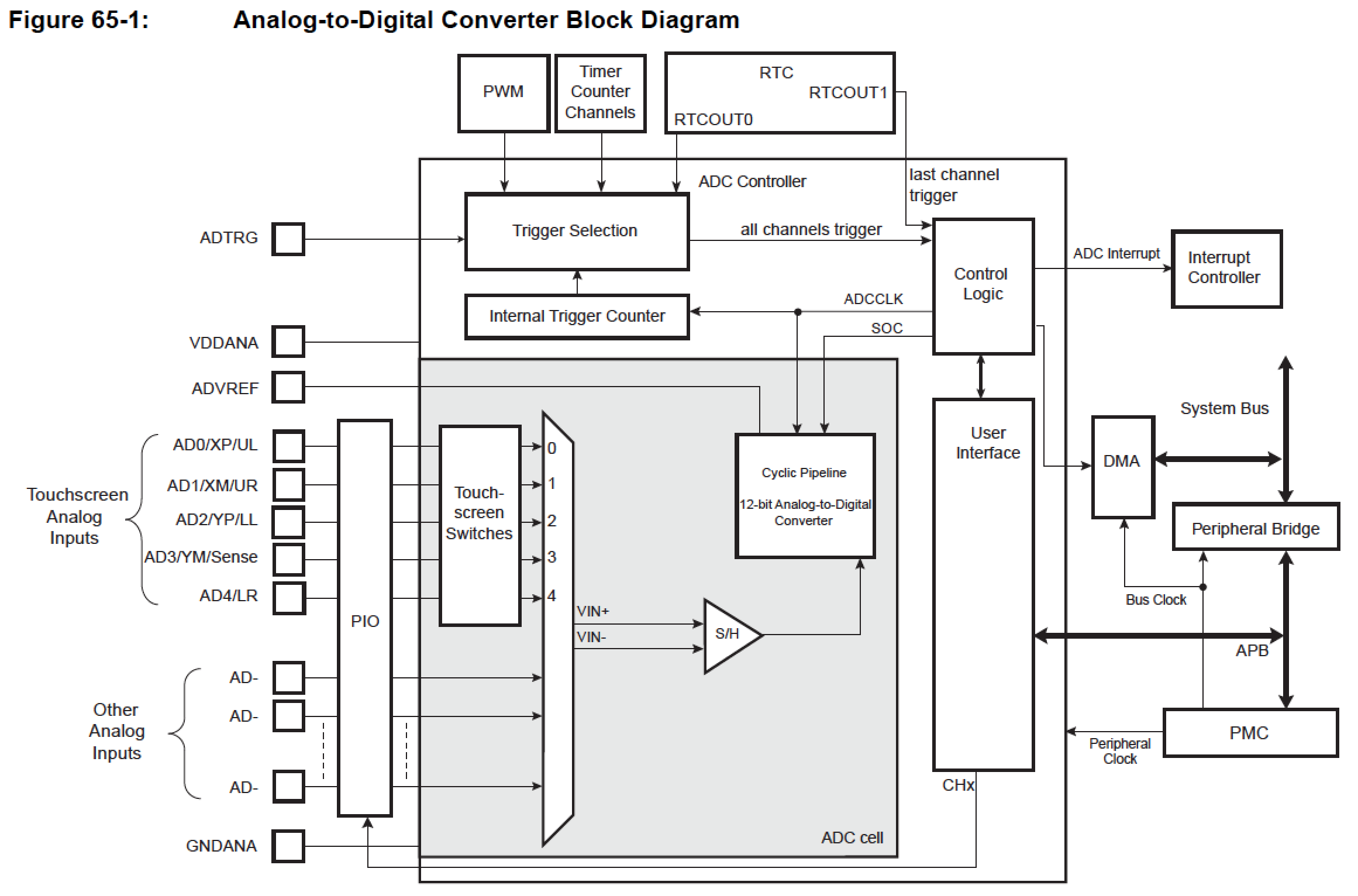
The ADC module of this MCU is based on a 12-bit Analog-to-Digital Converter (ADC) managed by an ADC Controller providing enhanced resolution up to 14 bits. It also integrates a 12-to-1 analog multiplexer, making possible the analog-to-digital conversions of 12 analog lines. The conversions extend from 0V to the voltage carried on pin ADVREF.
As explained in the SAMA5D2 Series datasheet
65.2 Embedded Characteristics
- 12-bit Resolution with Enhanced Mode up to 14 bits
- 1 Msps Conversion Rate
- Digital Averaging Function providing Enhanced Resolution Mode up to 14 bits
- Wide Range of Power Supply Operation
- Selectable class='acmetable' Single-Ended or Differential Input Voltage
- Digital correction of offset and gain errors
- Resistive 4-wire and 5-wire Touchscreen Controller
- Position and Pressure Measurement for 4-wire Screens
- Position Measurement for 5-wire Screens
- Average of Up to 8 Measures for Noise Filtering
- Programmable Pen Detection Sensitivity
- Integrated Multiplexer Offering Up to 12 Independent Analog Inputs
- Individual Enable and Disable of Each Channel
- Hardware or Software Trigger from:
- External Trigger Pin
- Timer Counter Outputs (Corresponding TIOA Trigger)
- ADC Internal Trigger Counter
- Trigger on Pen Contact Detection
- PWM Event Line
- Drive of PWM Fault Input
- DMA Support
- Two Sleep Modes (Automatic Wakeup on Trigger)
- Lowest Power Consumption (Voltage Reference OFF Between Conversions)
- Fast Wakeup Time Response on Trigger Event (Voltage Reference ON Between Conversions)
- Channel Sequence Customizing
- Automatic Window Comparison of Converted Values
- Asynchronous Partial Wakeup (SleepWalking) on external trigger
- Register Write Protection
The block diagram shows logic parts involved in A/D convertion and the name of the pins multiplexed for this purpose.

Table 65-1: ADC Pin Description
| Pin Name | Description |
|---|---|
| VDDANA | Analog power supply |
| ADVREF | Reference voltage |
| AD0–AD11 | Analog input channels |
| ADTRG | External trigger |
The ADC can be configured to operate in Single-ended mode (the default mode after a reset) or Differential mode. In Differential mode, the ADC requires differential input signals having a VDD/2 common mode voltage.
Please refer to Roadrunner pinout schematic and Roadrunner pinout table class='acmetable' for the position of the signals on the 2x100 pin connector.
I/O Lines
| Instance | Signal | I/O Line | Peripheral | Differential mode |
|---|---|---|---|---|
| ADC | ADTRG | PD31 | A | |
| ADC | AD0 | PD19 | X1 | CH0 |
| ADC | AD1 | PD20 | X1 | CH0 |
| ADC | AD2 | PD21 | X1 | CH2 |
| ADC | AD3 | PD22 | X1 | CH2 |
| ADC | AD4 | PD23 | X1 | CH4 |
| ADC | AD5 | PD24 | X1 | CH4 |
| ADC | AD6 | PD25 | X1 | CH6 |
| ADC | AD7 | PD26 | X1 | CH6 |
| ADC | AD8 | PD27 | X1 | CH8 |
| ADC | AD9 | PD28 | X1 | CH8 |
| ADC | AD10 | PD29 | X1 | CH10 |
| ADC | AD11 | PD30 | X1 | CH10 |
Electrical interface
The maximum voltage level that can be applied to an analog input must be equal or lower than the analog voltage power supply: VADVREF.
66.10.2 External Reference Voltage
VADVREF is an external reference voltage applied on the pin ADVREF. The quality of the reference voltage VADVREF is critical to the performance of the ADC. A DC variation of the reference voltage VADVREF is converted to a gain error by the ADC. The noise generated by VADVREF is converted by the ADC to count noise.
Table 66-29: ADVREF Electrical Characteristics
| Symbol | Parameter | Conditions | Min | Typ | Max | Unit |
|---|---|---|---|---|---|---|
| VADVREF | Voltage Range | Full operational | 2 | – | VDDANA | V |
| VADVREF | RMS Noise | Bandwidth 10 kHz to 1 MHz | – | – | 100 | μV |
| RADVREF | Input DC Impedance | ADC reference resistance bridge | 6 | 8 | 10 | kΩ |
| IADVREF | Current | VADVREF = 3.3V | - | - | 460 | μA |
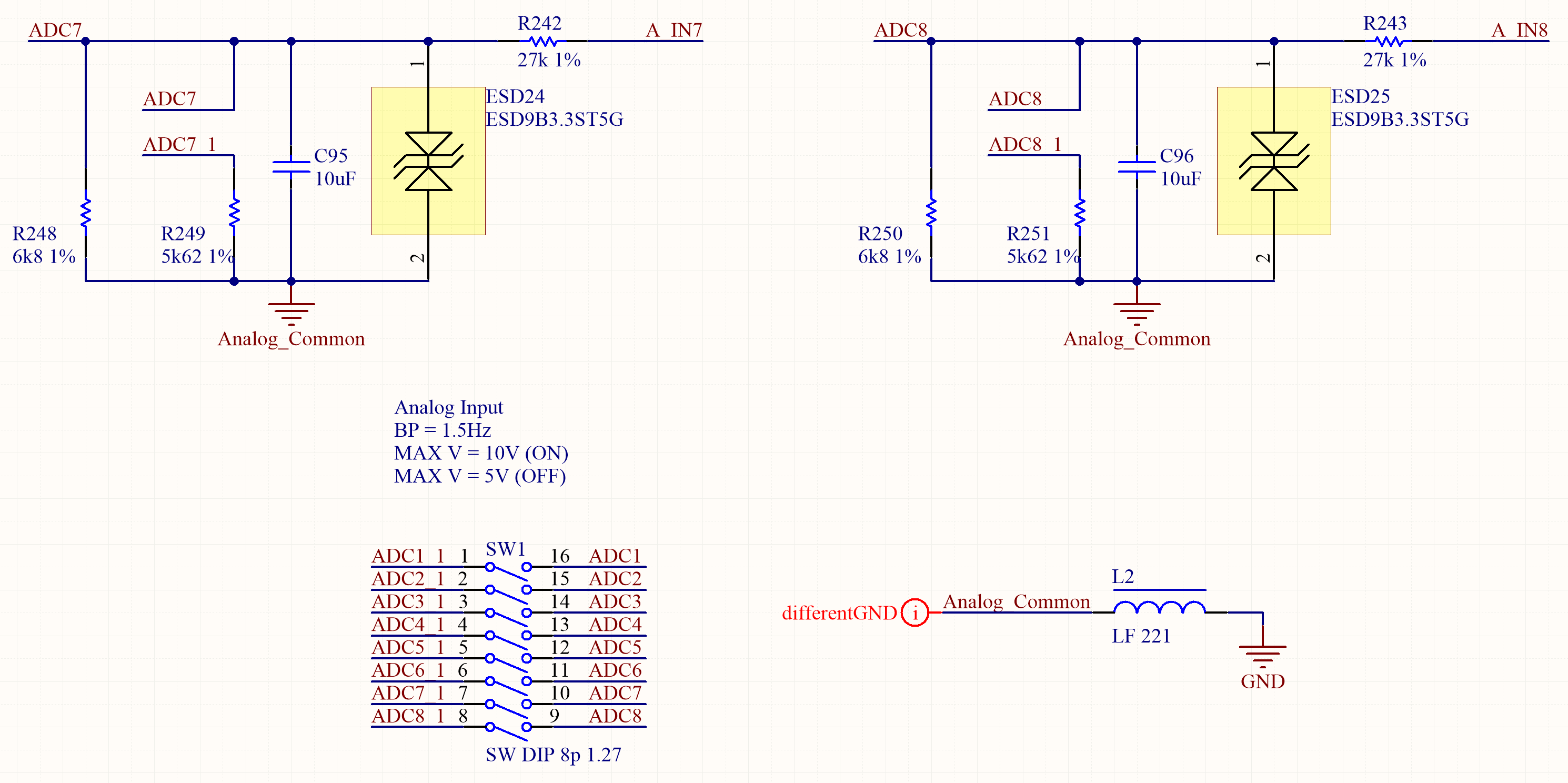
Because of these constraints the voltage under measure must be well conditioned before being applied to the ADC pin. In the schematic example below there is a Transient Voltage Suppressor that, together with the input series resistor, limits the maximum voltage for both permanent signals or spikes (ESD). In this example the reference voltage is 1V. A voltage divider is applied to extend the measurement range. Two different full-scales, 5 or 10V, can be selected inserting different resistors with the switch. The low-pass RC filter composed by the input resistor and the capacitor limits the frequency, and therefore the noise, to 1.5Hz, usefull to measure slow fluctuating signals as a power supply voltage or temperature sensors.

Output Impedance
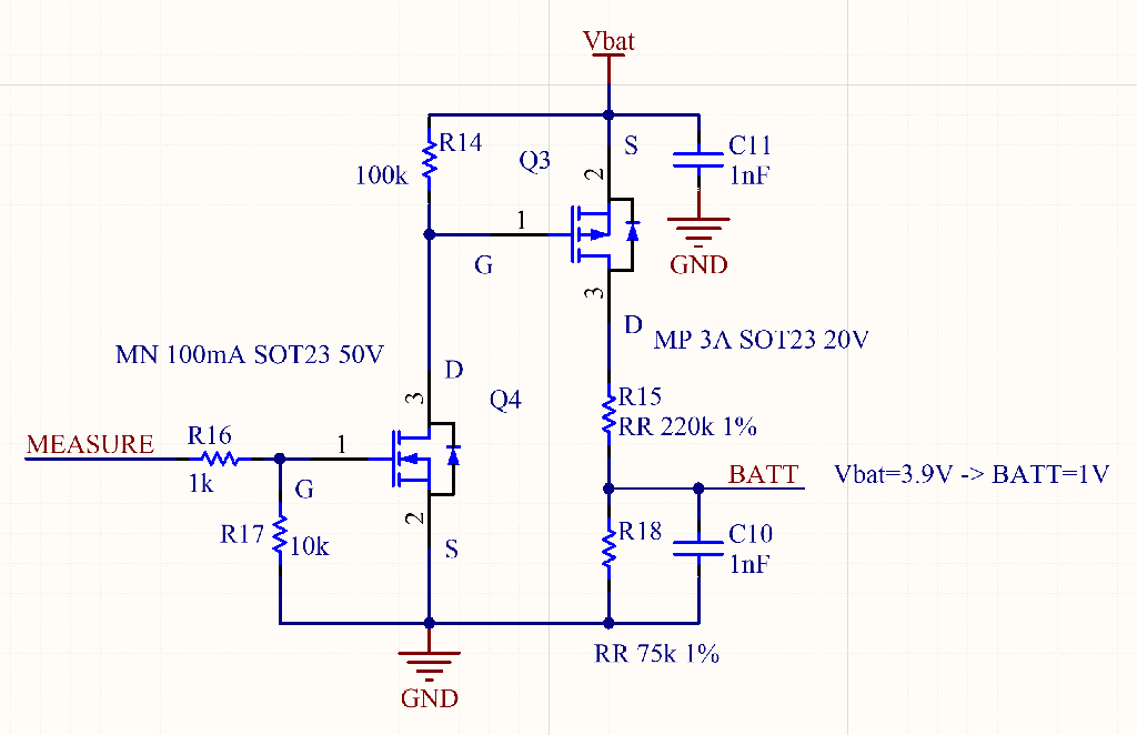
Which is the right value for the output impedance of the circuit under ADC measurement? We can find a lot of rules-of-thumb looking around: 1kΩ, 10kΩ, 100kΩ, less is better. Yes, less is better, but how much less? Usually the need is to acquire a large amount of samples in order to reproduce a variable signal with the best possible quality, according to the Nyquist-Shannon sampling theorem. To obtain the maximum possible sampling rate, sometimes it requires an active amplifier (such as an emitter follower, a common drain or a unity gain op-amp buffer) to low down the output impedance of the circuit. But there are some specific cases where a low impedance not only is not required but it is also harmful, e.g.: measuring the charge status of a battery. The battery voltage must be conditioned with a resistor divider to fit the ADC range. It could be enough to measure the voltage level once or twice a minute, the signal changes slowly, but we cannot continuously drain a significant amount of current on the divider to avoid a high self-discharge rate. If the battery is a coin cell that has to last for years in an IoT device, It is advisable to measure the voltage level once or twice a day. In this very extreme case it could be necessary to add a circuit that connects the resistors only when needed and detaches them after the measure, such in this schematics:

In some cases the circuit can be simplified avoiding the switch but using a value of MΩ for the resistors, introducing a drain of some µA or less. To have the ADC working correctly with such high values we need to configure the ADC register differently from the default. Let's understand how the ADC circuitry works to know how it has to be setup and why.

Most of the ADCs use a sample & hold system for the input circuit as in the example above. A capacitor (Cpin) is connected to the input for a specific time (acquisition time), than it is detached and the sampled voltage is measured with one of the standard ways (simple or dual slope, SAR, ΣΔ, or whatever) measuring the discharging time on a known resistor (conversion time) with a 6 to 24 bit resolution. Then the capacitor is completely discharged short circuiting it. The sum of all of those times is the full sampling time that is responsible of the maximum sampling rate. The whole cycle is clocked by the ADC clock, derived from the main MCU clock through a divider. On the smaller MCUs the cycle phases must be triggered by the user firmware polling for a flag or waiting for an interrupt. On bigger and newer MCUs all the process is performed automatically at the maximum speed, often also using the DMA to free up the CPU from trivial tasks.
Usually the time is computed as a certain number of clock ticks. The only time useful to calculate the output impedance is the acquisition time. The output impedance and the S&H capacitor form an RC circuit with a known time constant, we have to setup the acquisition time lasting enough to full charge the capacitor. The ADC peripheral registers of the MCU must be configured to have a very low clock and a very high acquisition time. In this way we can also use an output impedance of some MΩ with a correct reading.
