How to design the power supply circuitry
Introduction
Let's introduce some attentions that must be applied on every circuit, common to all the projects described below.
As explained in the SAMA5D2 Series datasheet Table 66-3: DC Characteristics, the different power supplies needed for the MCU operation can admit a ripple level well within the characteristics of many actual switching regulators. This kind of regulators right now are cheap, require a limited number of external components, have high efficiency and low ripple. Therefore, except in some very specific situations, they are more advisable than the classic linear regulators which waste a lot of energy.
Calculating the right values for compensation network and filtering devices is not a very easy task, but many producers publish design tools that simplify a lot the choice of the external components in every specific application. One example is the Texas Instruments WEBENCH® Power Designer. Those tools return even a detailed BOM of the circuit with links to a set of suggested suppliers. The quality of the components may influence a lot how the switching regulator works. Despite the advantages of ceramic capacitors, care must be taken during the design process to ensure stable class='acmetable' operation over the full operating voltage and temperature range. Ceramic capacitors are available in a variety of dielectrics, each of which exhibits different characteristics that can greatly affect performance over their temperature and voltage ranges. Two of the most common dielectrics are Y5V and X5R. Whereas Y5V dielectrics are inexpensive and can provide high capacitance in small packages, their capacitance varies greatly over their voltage and temperature ranges and are not recommended for DC/DC applications. X5R and X7R dielectrics are more suitable class='acmetable' for output capacitor applications, as their characteristics are more stable class='acmetable' over their operating ranges, and are highly recommended. The inductor must have a low DC-resistance, and DC ratings that exceed the maximum output current by at least 30% to avoid inductor saturation. Correctly choosing the right values for capacitors and inductors makes the circuit more stable class='acmetable', but a good PCB design is still essential to avoid high ripple or even self-oscillations.
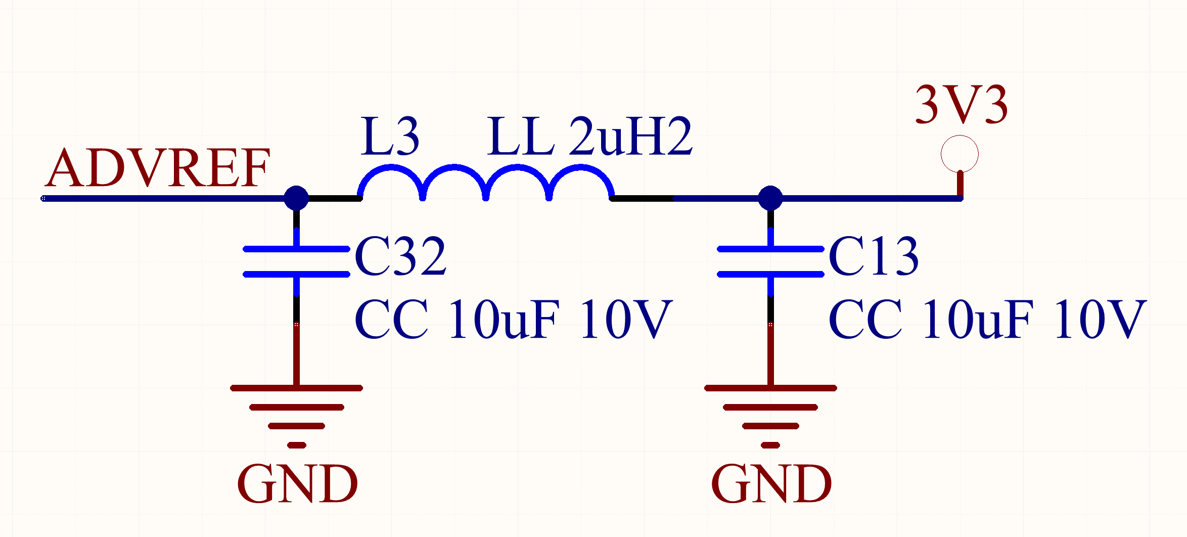
More ripple sensitive power supplies of the MCU (e.g.: analog voltage reference) can be better protected by adding a PI filter.
Only when very high noise immunity is necessary, as in converting very low-level analog signals, a cascading LDO regulator could be needed to filter out all the ripple.
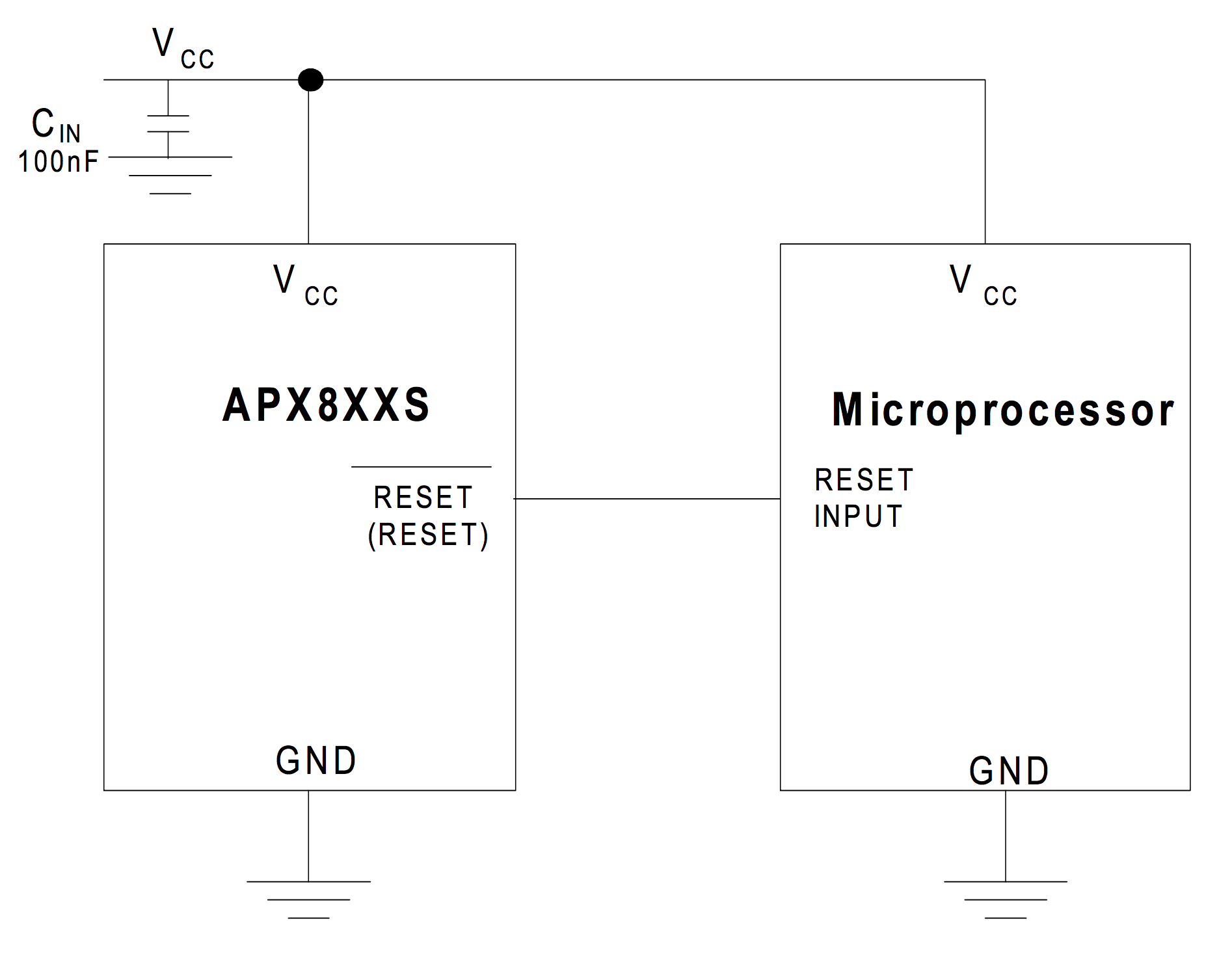
To be sure that the whole set of SAM5D27 MCU peripheral can operate correctly, it's better to supply the MCU with an at least 3V power supply, even if some parts work also with a lower voltage. But an instable class='acmetable' supply, that varies up during the power-on or down during the power-off, can lead to unpredictable class='acmetable' behaviors of all the system. Many other devices connected to the MCU can go crazy as well in such conditions. To prevent this kind of problems a power supply supervisor is implemented in the Roadrunner SOM. A simple 3-PIN MICRO POWER VOLTAGE DETECTOR APX809-31SAG-7 asserts a reset signal whenever the VCC supply voltage declines below 3.08V, keeping it asserted for at least 240ms after VCC has risen above this reset threshold. This control signal is directly connected to the NRST pin of the MCU and is available too on J1-24 pin of the SOM connector to also reset sensitive external devices such, for example, SD cards.
The 3V3_OUT pins of the connector carry out the 3V3_IN power supply through a mosfet controlled by the MCU. When the MCU goes off, it's therefore possible to switch off too external devices like, for example, ethernet PHY, to guarantee a real zero current power off.
Let's now explain some real working projects designed for different situations.
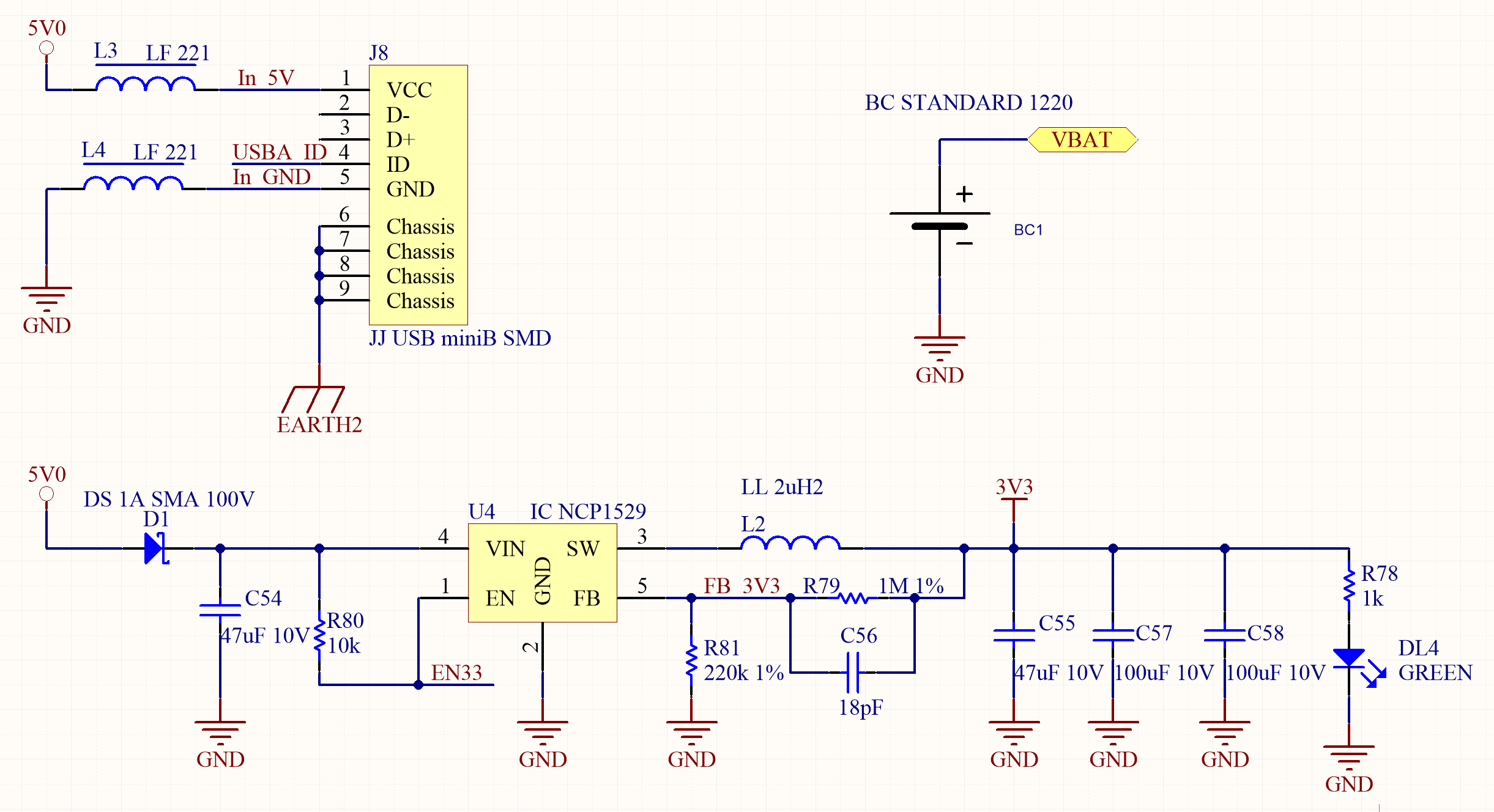
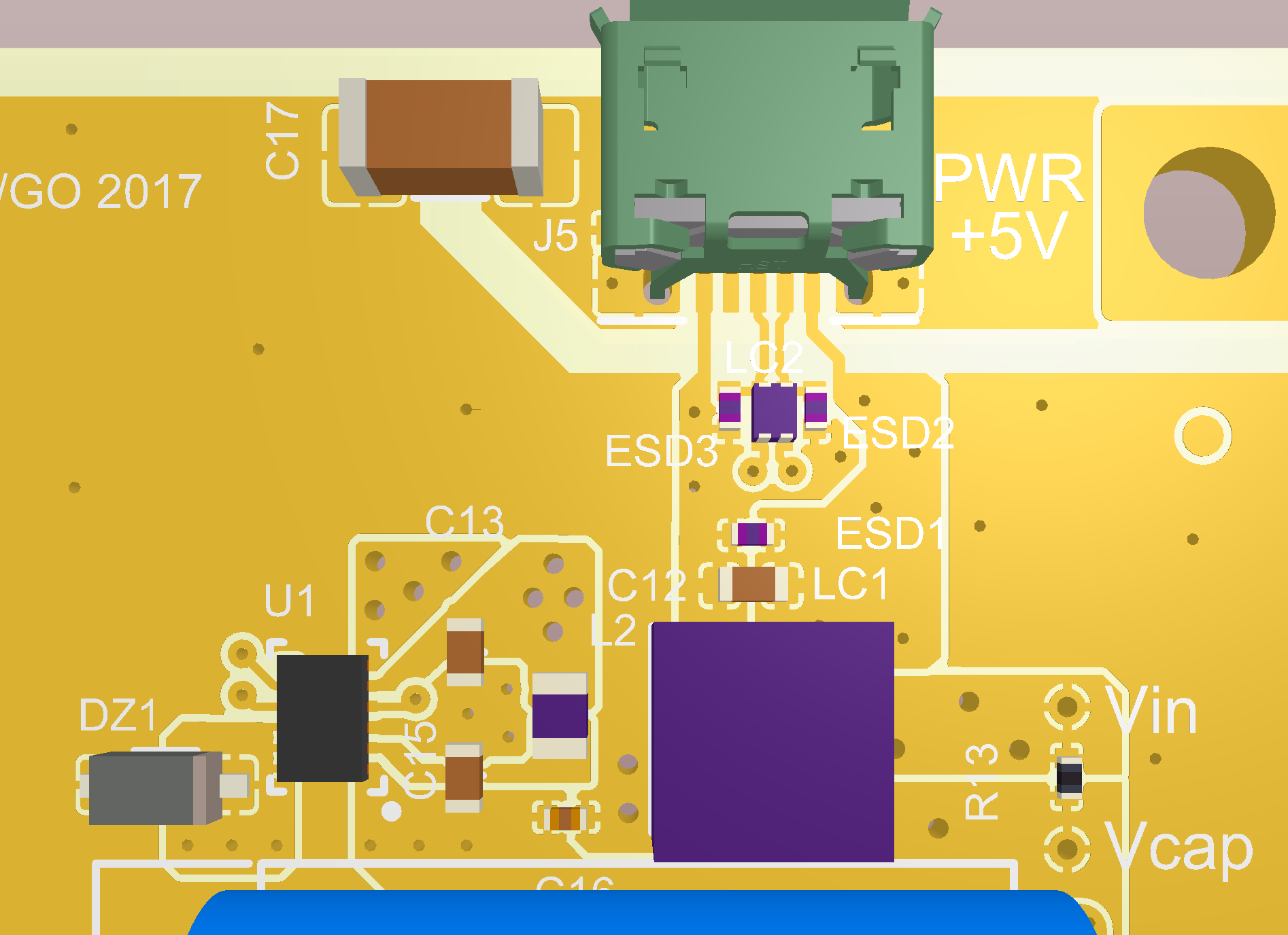
Example 1: Standard 5V power supply from USB connector
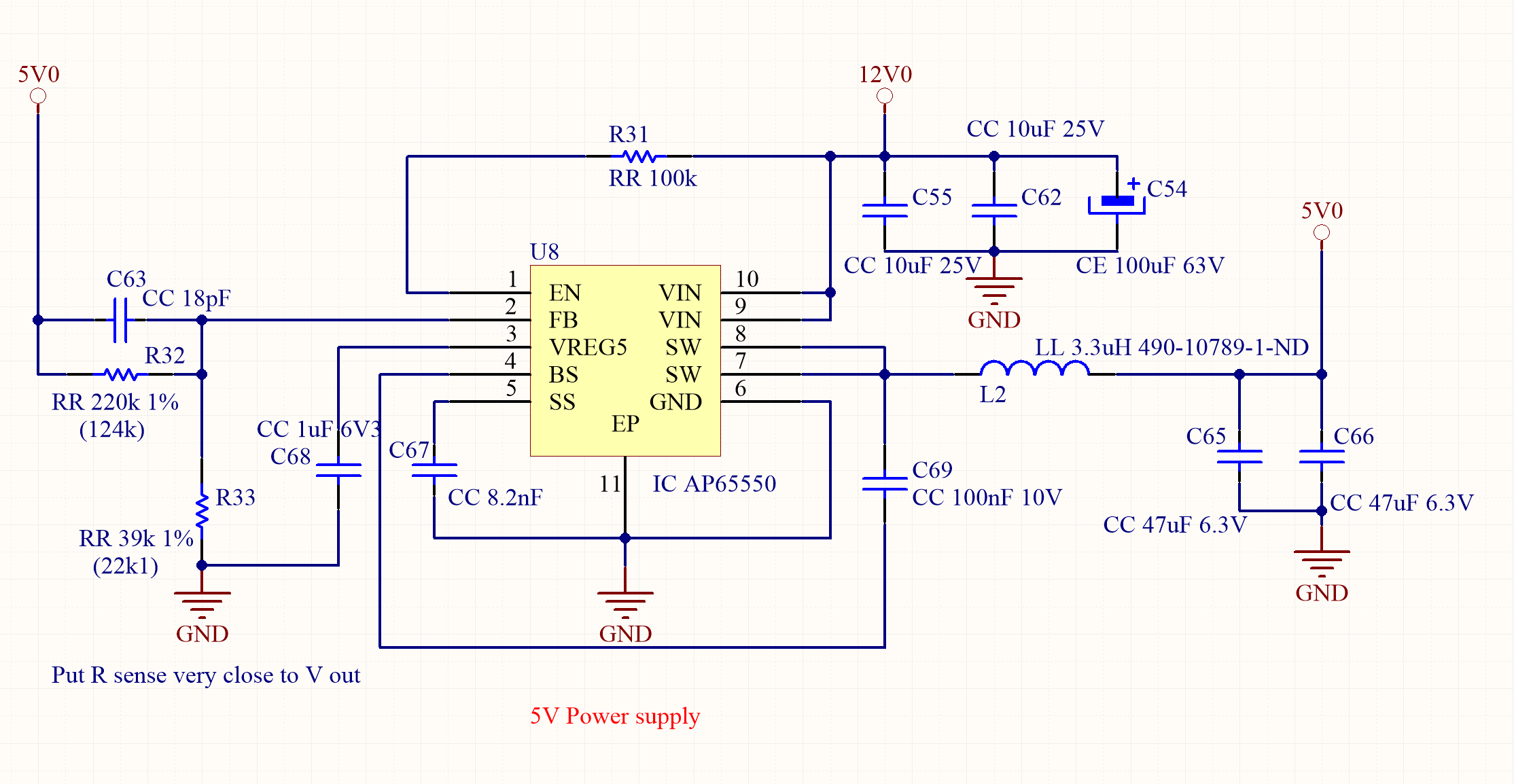
The first example is the most common situation: a 5V external power supply, often coming from an USB cable connected to an host device or to a simple wall power adapter. The NCP1529 1A switching regulator has enough capabilities to supply the Roadrunner plus some other external device, low external components count, a small footprint also because of the 1.7MHz switching frequency that allows small inductors and capacitors.
An external battery allows the MCU to work in backup mode. It's connected to Vbat pin of the Roadrunner connector and powers up the Vddbu section of the SAMA5D27. The data sheet Table 66-14: Typical Power Consumption for Backup Mode helps on calculating the right battery capacity needed to have the wanted backup autonomy without main power supply.
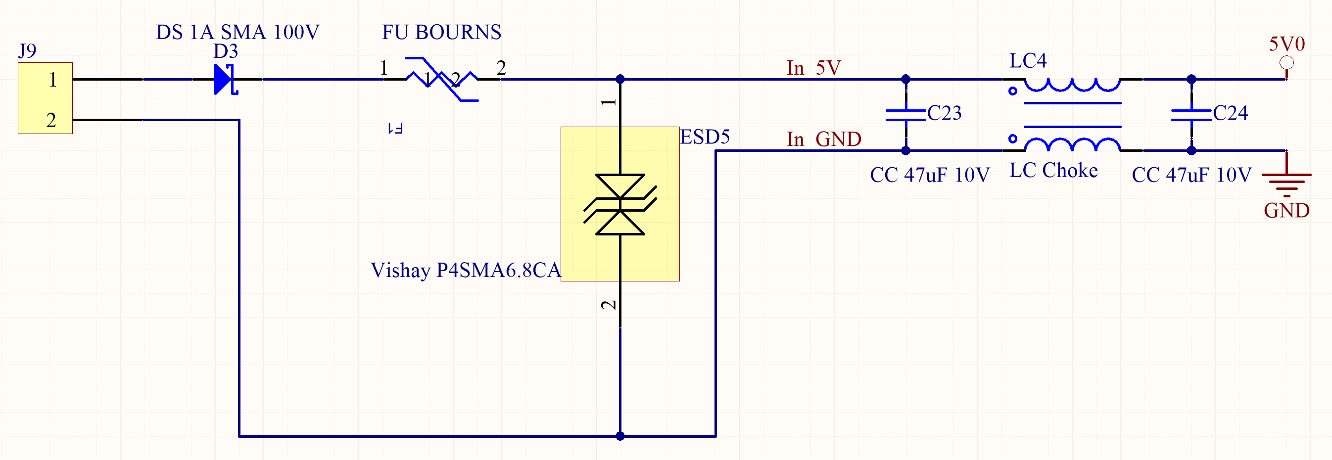
If the 5V power supply is not reliable enough, it's better to add some protection and filtering devices.
The polarity inversion is protected by a Schottky diode to minimize voltage drop compared to a standard diode. Possible overvoltage, as well as ESD, is cut off by the Transient Voltage Suppressors together with the resettable class='acmetable' fuse. If the voltage, continuously or in just a peak, goes over the TVS threshold this starts conducting; when the circulating current exceeds 1A the fuse opens the circuit until the condition comes back within normal values.
The low pass filter formed by the common mode choke and the capacitors blocks both the radiated and conducted emissions.
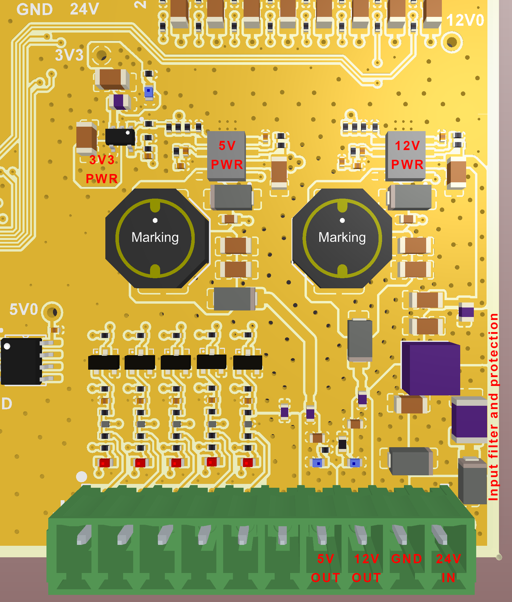
Most of the ripple on the output voltage is due to the parasitic resistance of the LC filter. A very low ESR ceramic capacitor is strongly suggested as well as a low resistance inductor. But also the impedance of the PCB tracks between this components and the IC must be lowered as much as possible to have both good efficiency and low ripple. As shown on the PCB routing example below, those components must be placed as close as possible to the IC pads and connected together through generous polygon planes. The ground return paths must be kept at the lower possible impedance using a good number of vias to connect the upper to the internal ground planes. The regulator switches at an high frequency with sharp edges and a lot of energy. This causes a wide spectrum of frequency that forces to design the PCB with concept similar to an RF circuit. Once more a sufficient amount of vias it's important to short the top ground to the bottom ground in order to reduce the return path and decrease the radiated emissions. Even if a good design can guarantee a suitable class='acmetable' ground plane closely below the top layer also with a two layer PCB, a 4 or more layer stack helps a lot on having a power supply with almost ideal characteristics and EMC constraints compliant.
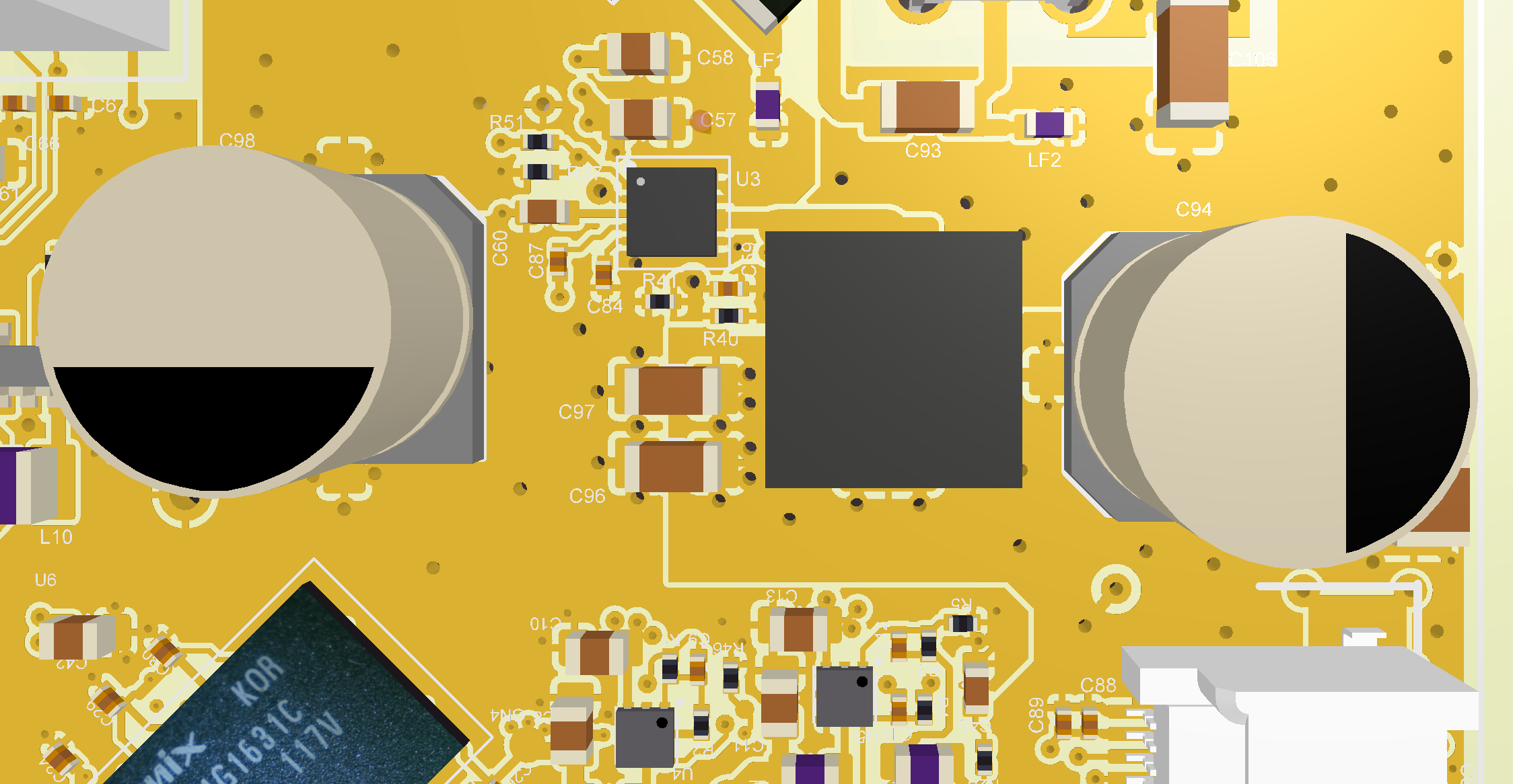
Example 2: Separated power supply for heavy load devices on the same board.
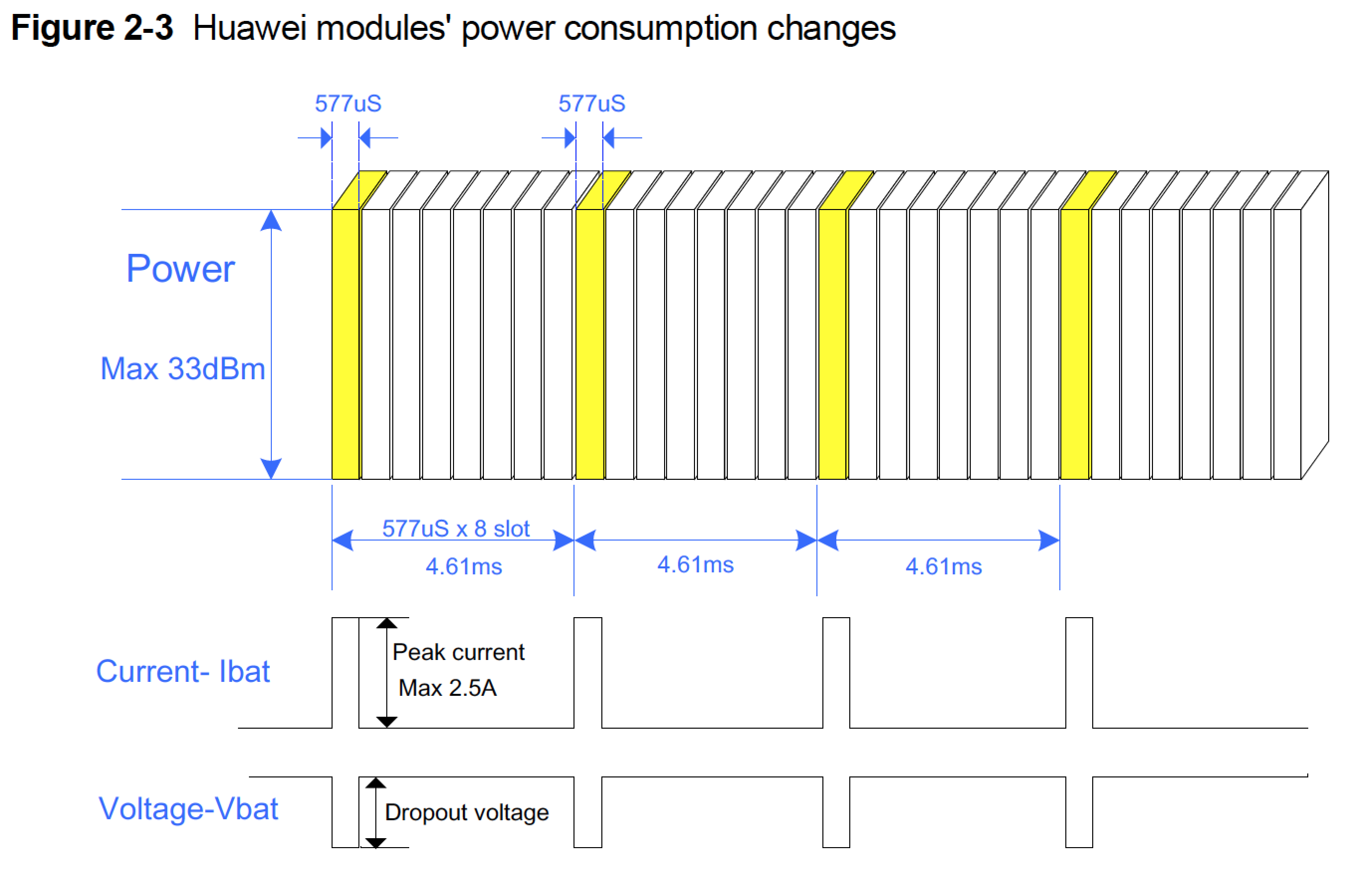
One or more power hungry devices can operate on the same board of the MCU. An example is an high-speed communication modem. As specified in a typical HSPA+ Mini PCIe Module datasheet, in some specific conditions the peak current may reach a very high level, even if just for a short period. If the power supply does not have good transient response performance, this can cause a voltage drop with an unpredictable class='acmetable' behavior.
In order to have a good transient response we need a power supply with enough capacity to store the energy required during the peaks, and the impedance of the PCB must be very low. When possible it's better to use a power supply for this section separated from the MCU one. This allows two different power supply designs, each specialized for its own application and physically placed closer to the utilizer, reducing a lot possible interference between them. Furthermore, in this way the MCU can control this separated power domain switching it on only when needed.
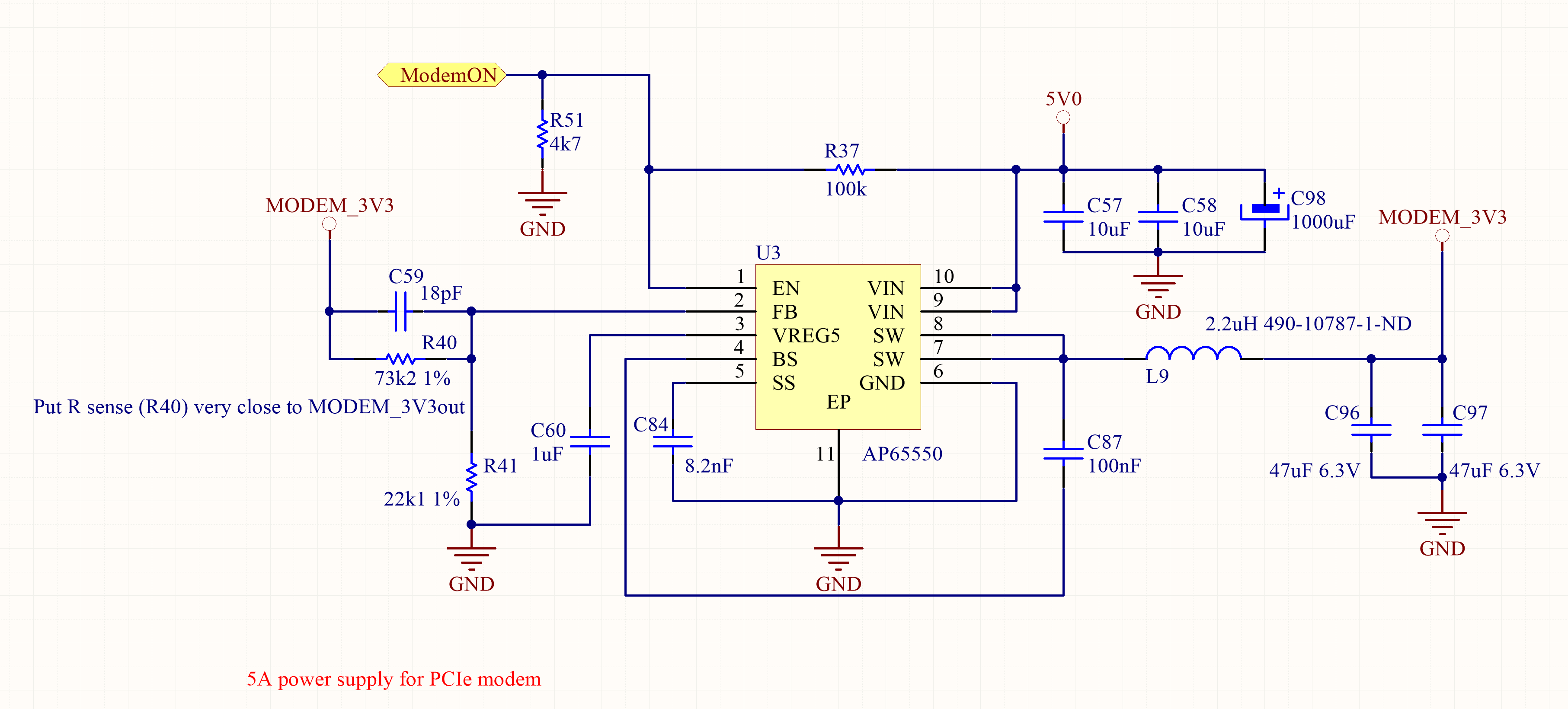
An AP65550 step down converter is used in this case. In addition to its 5A capability it can be powered up to 18V, allowing the design of a power supply with a wider input voltage range than the NCP1529. The drawback is a greater footprint because of lower operating frequency that requires more generous inductors and capacitors.
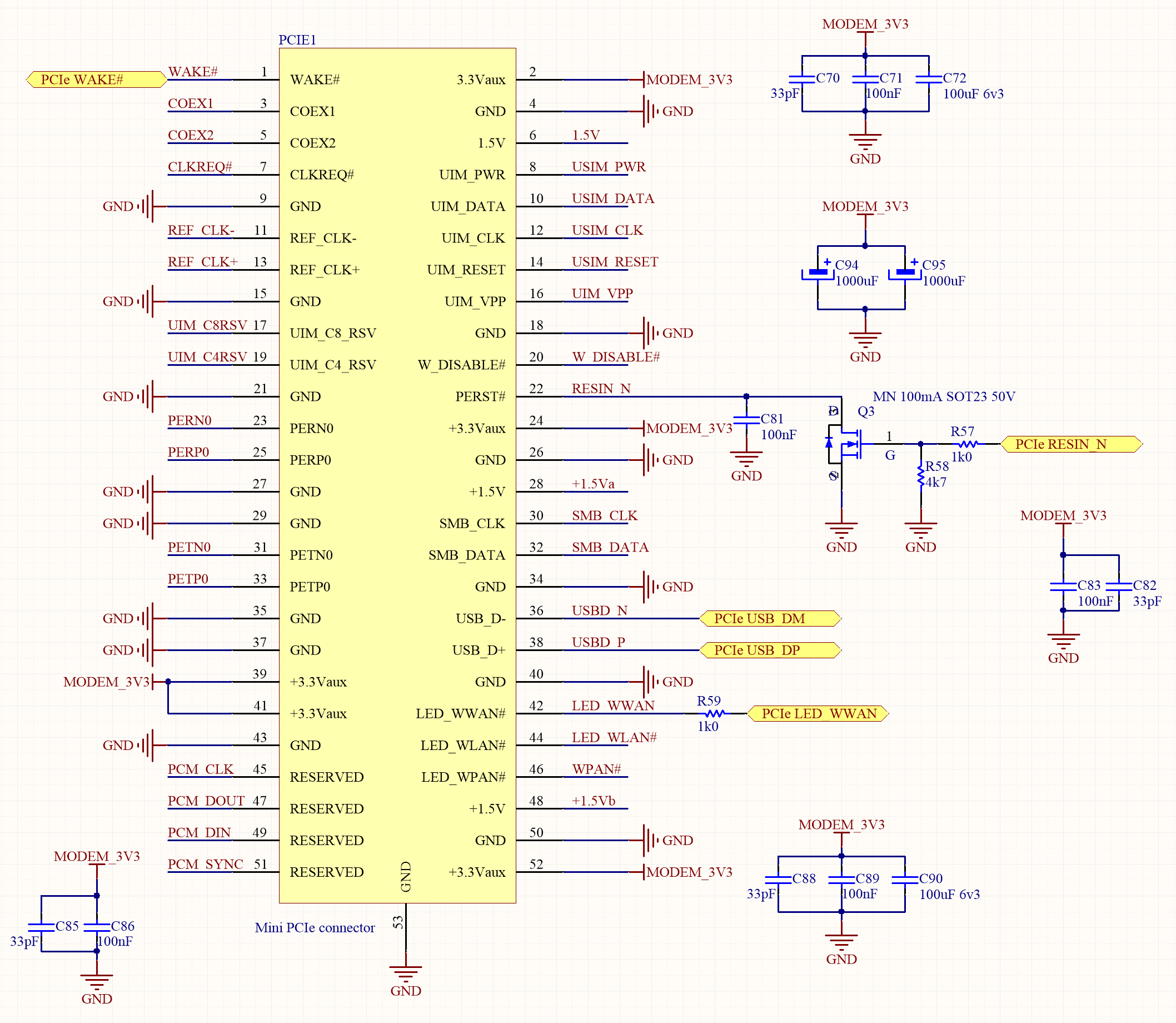
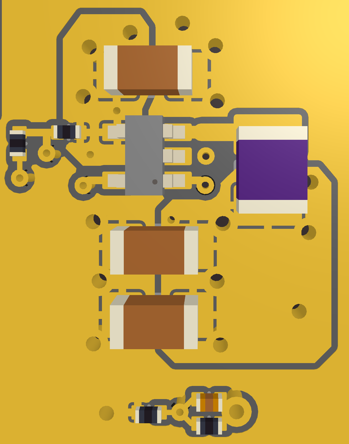
The schematics and the PCB routing show how many capacitors are distributed on the circuit. Most of them are placed very close to the power input pins of the PCIe modem, to minimize the tracks impedance. The 1000μF capacitors supply the energy reserve to react to the power transients. The 100nF capacitors filter out high frequencies and the 33pF capacitors filter out the very high frequencies generated by this communication device.
In the picture below is evidenced the voltage sensing track routed on an internal layer. This is the feedback that enables the regulator to maintain the correct voltage. Catching the output voltage very close to the power user, guarantees a better regulation compensating the voltage drop due to the PCB track impedance between the regulator and the load.
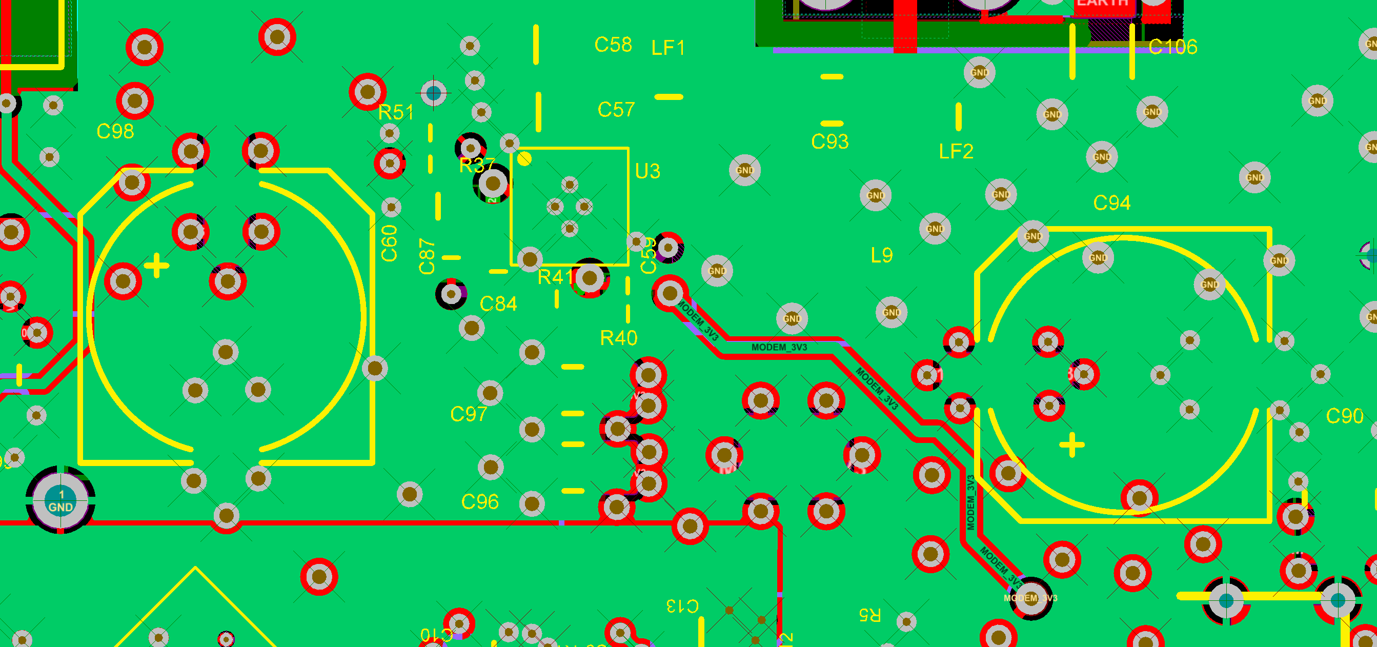
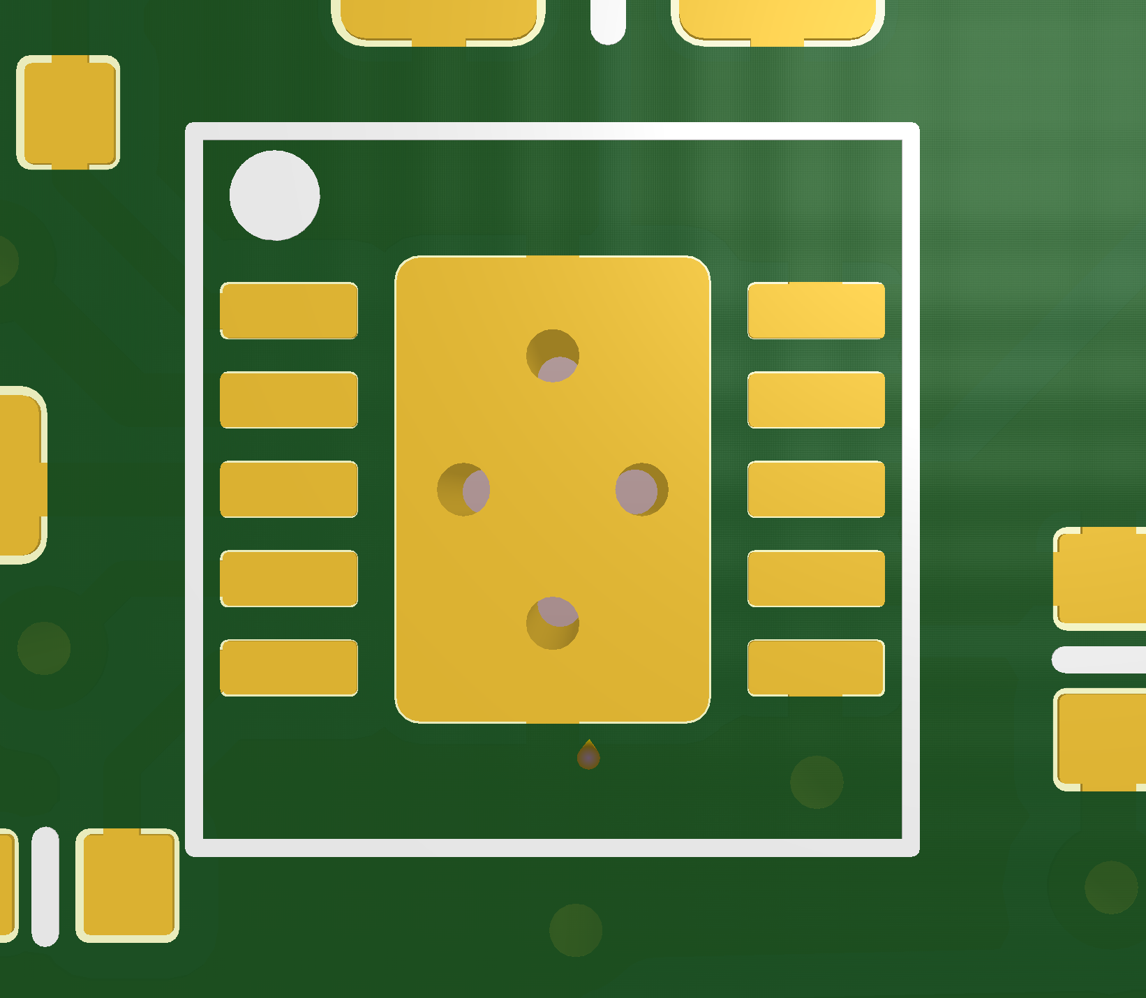
Very often the regulators have a big exposed pad at the bottom of the package. This is essential to guarantee a good contact with the ground plane from both electrical and thermal point of views. A good amount of vias is strongly recommended to allow a good heat dissipation on the lower layers.
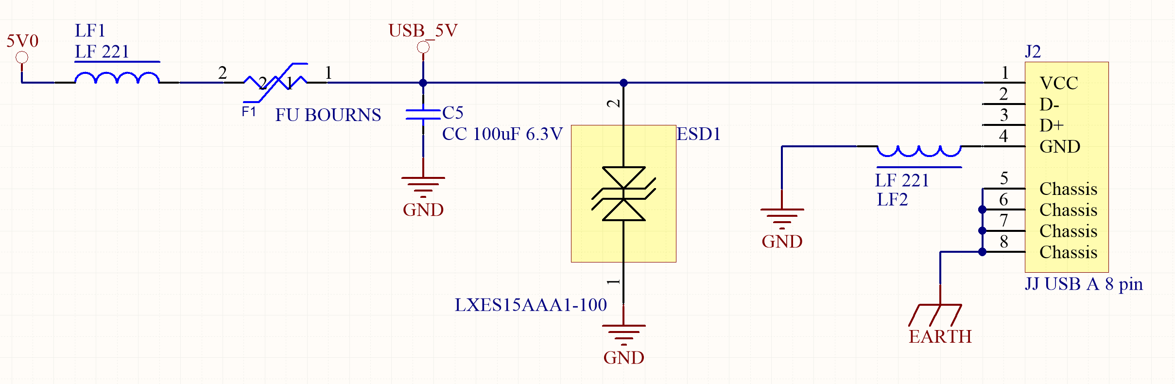
Example 3: 12V input with additional 5V out to power up external USB devices
In this example an AP65550 regulator is used to generate a 5V power supply if on the board is placed an USB host interface that powers up external devices. The main voltage can be up to 18V and the MCU can be powered cascading a little NCP1529 from the 5V as done in the example 1.
A protection from external devices interferences and current overload must be added between the power supply and the USB type A host connector.
Example 4: 24V input with multiple external power supply out
In an industrial environment it's often used a main power supply of 24V to reduce current requirements and consequently the wires size. The previous regulators cannot be used because of their voltage limits. Here an example with the TPS54231 28-V Input, Step-Down DC-DC Converter. The multiple output voltage is required by the project to power up external devices. Because those power supplies is connected to the world outside, the internal components must be well protected from reverse voltage and EMI with diodes and LC filters. The input supply as well is protected with a circuit similar to the one described in example 1. Once again the MCU 3.3V power supply comes from a tiny NCP1529 powered by the internal 5V.
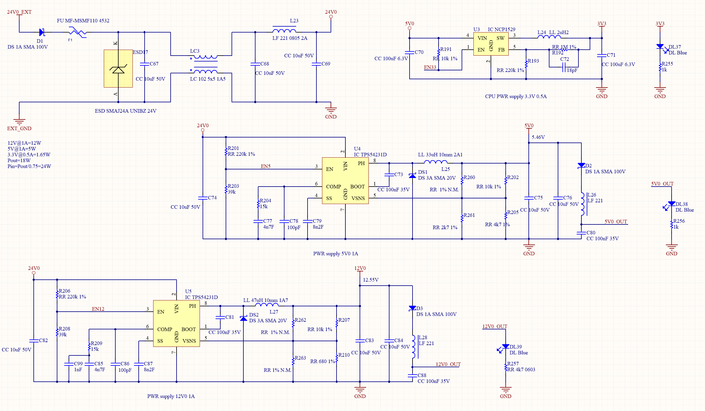
The TPS54231 works at 500kHz, therefore it requires a quite big inductor and an external catch diode. This increases the footprint on the PCB, but the regulator is very stable class='acmetable' and with low ripple. The path for the switching current is localized among the regulator, the LC filter and the catch diode. All of these components PCB design requires the attention for track impedance and ground plane already described. Note on this picture the amount of big vias placed to shield the regulators area around and below with uninterrupted ground planes.
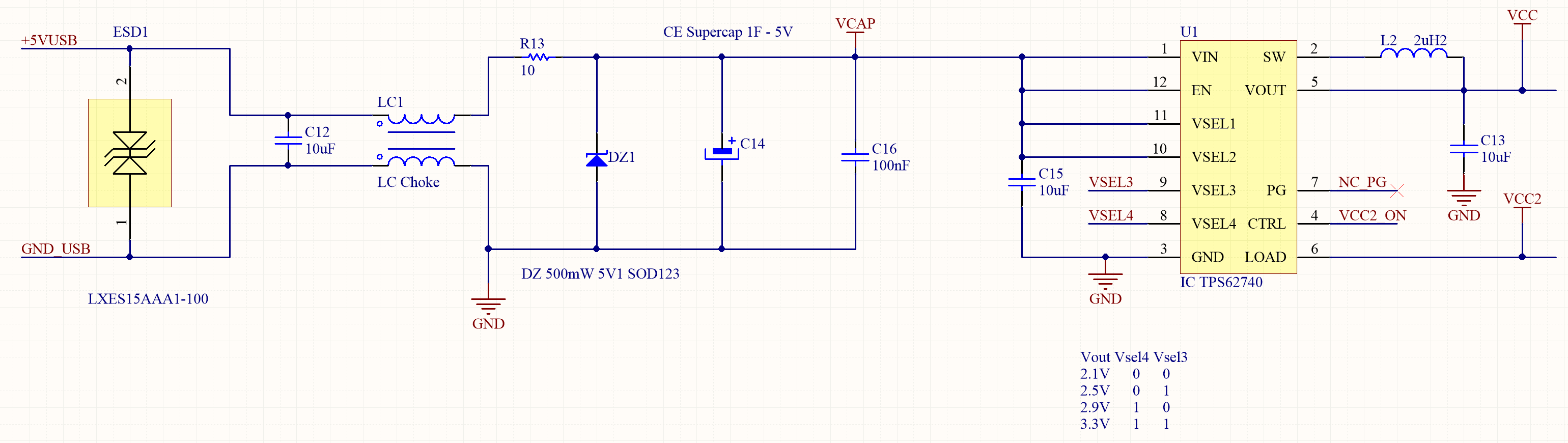
Example 5: very low power with energy harvesting capabilities
Some ideas to wonder on very low consumption system powering can be get by another article regarding Long lasting battery solution
Here is used a very low quiescent current, software selectable class='acmetable' Vout, step down converter for low power applications TPS62740
Related links
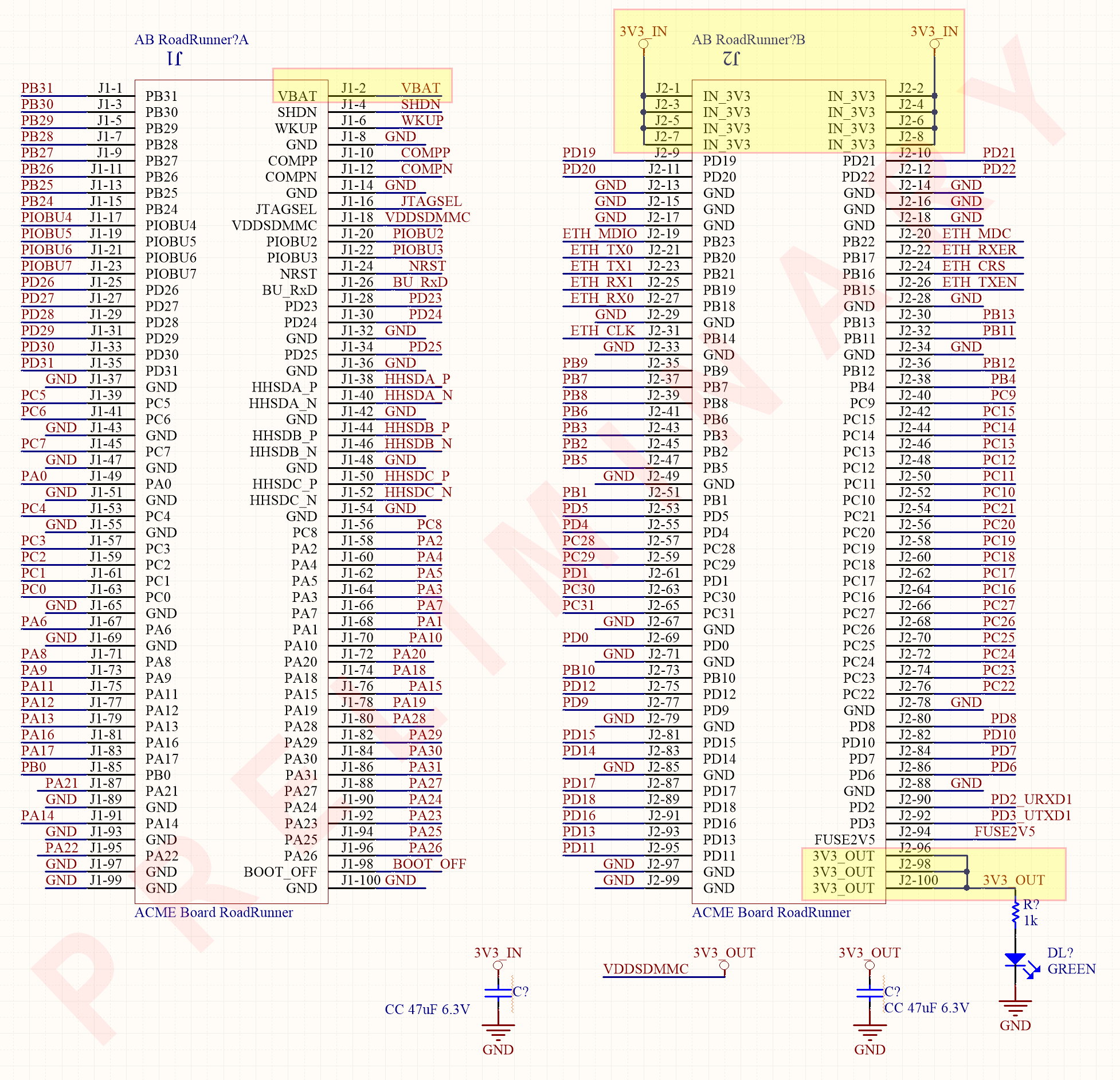
- Roadrunner power pinout (PRELIMINARY)
- Roadrunner power requirements
- SAMA5D2 Series datasheet
- APX809S 3-PIN MICRO POWER VOLTAGE DETECTOR
- NCP1529 1.7MHz, 1A, High Efficiency, Low Ripple, Step-down Converter
- AP65550 5A, 18V, 650kHz ADAPTIVE COT STEP-DOWN CONVERTER
- TPS54231 2-A, 28-V Input, Step-Down DC-DC Converter With Eco-mode
- TPS6274x 360nA IQ Step Down Converter For Low Power Applications
- Texas Instruments WEBENCH® Power Designer.
