Roadrunner technical documentation
Roadrunner pins description
Introduction
Let's divide the pins in five logical groups.
They are highlighted with different colors in the diagram below (click to enlarge).
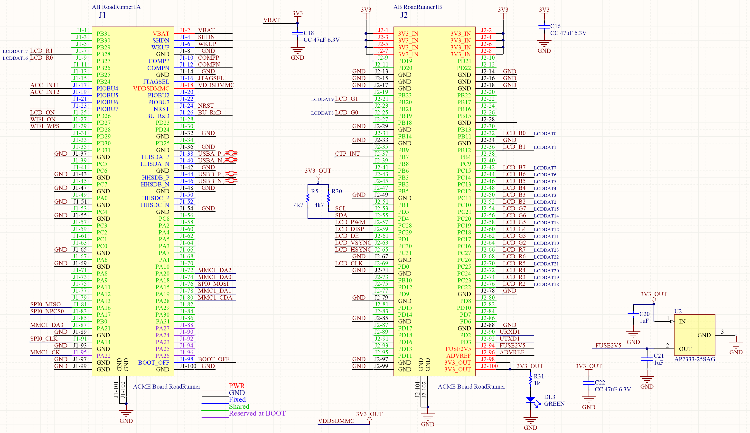
The schematic diagram also shows some connections on the shared pins as an example for the most commonly used peripherals.
PWR
This group collects all the pins related to the power supply.
3V3
The 3V3 power supply must be applied to pins J2-1 to J2-8. The requirements and suggestions to design a reliable power supply are available on How to design the power supply circuitry document. The voltage level is supervised to be within the correct range by a circuit internal to the SOM as described here. All the other circuits needed to generate and control the correct voltages in the right power-up and power-down sequence requested by the MCU, are optimized on the SOM.
VBAT
The SAM5D2 has many different power saving modes, offering the best compromise between responsiveness and power consumption in different situations.
SAMA5D2 devices feature three software-selectable class='acmetable' low-power modes: Idle, Ultra-low-power and Backup.
In Idle mode, the processor is stopped while all other functions can be kept running.
In Ultra-low-power-mode 0, the processor is stopped while all other functions are clocked at 512 Hz and interrupts or peripherals can be configured to wake up the system based on events, including partial asynchronous wakeup (SleepWalking).
In Ultra-low-power mode 1, all clocks and functions are stopped but some peripherals can be configured to wake up the system based on events, including partial asynchronous wakeup (SleepWalking).
In Backup mode, RTC and wakeup logic are active. The Backup mode can be extended to feature DDR in Selfrefresh mode.
SAMA5D2 devices also include an Event System that allows peripherals to receive, react to and send events in Active and Idle modes without processor intervention.
The Battery IN voltage is required if the circuit needs the whole set of features related to Backup mode. Please look at the VDDBU details on SAMA5D2 Series datasheet for a correct optimization of the low power features of the MCU.
The simplest way to enable the Backup mode features is supplying the VBAT power with just a coin battery
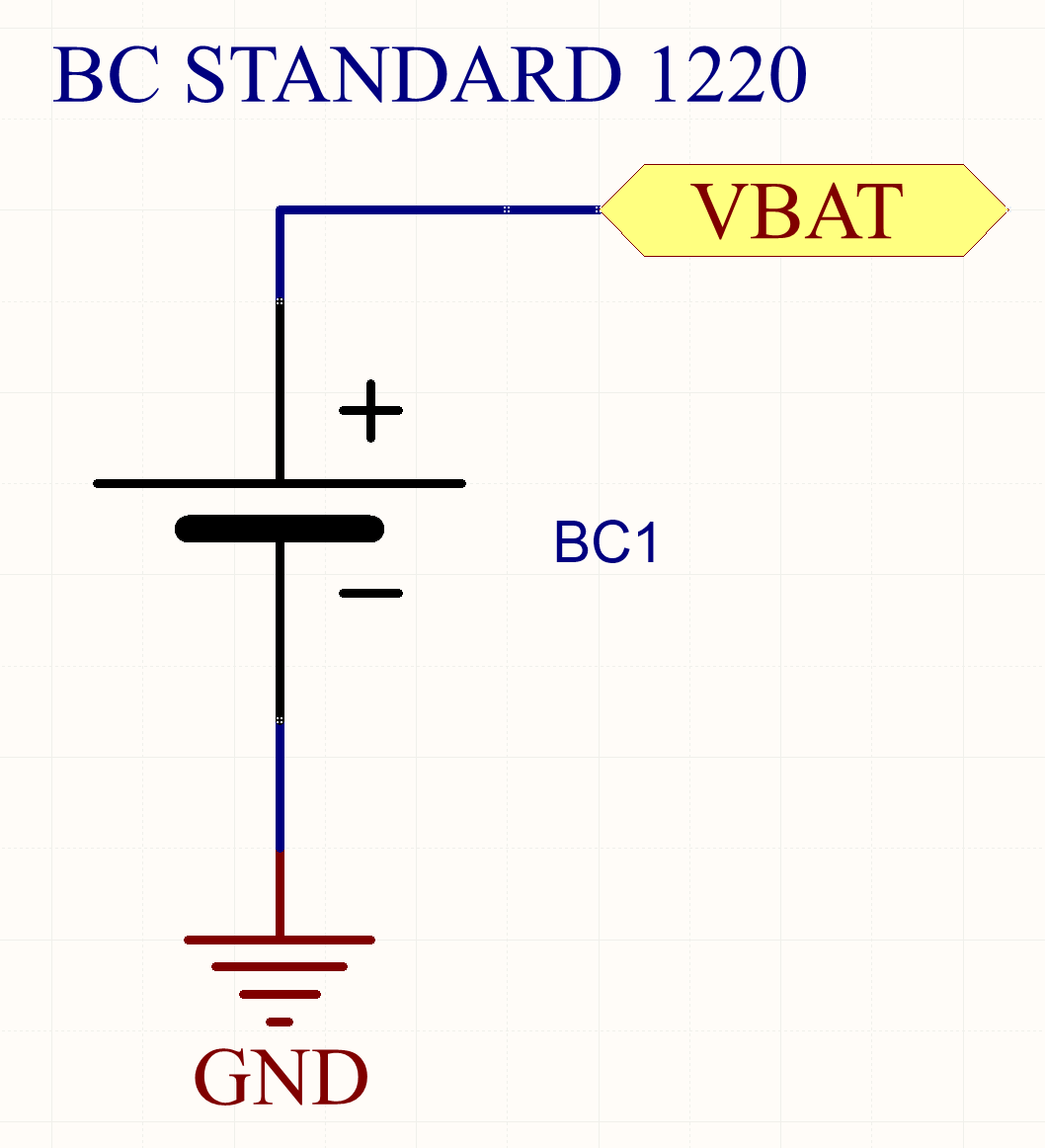
The voltage must not exceed the Absolute Maximum Rating of 4.0V. Operating voltage is between 1.65 and 3.6 V, with a typical consumption of 4.5 μA in backup mode at 25°C/3.0V.
For a more environmental safe mode, with fewer problems for storing and transportation restrictions, the battery could be substituted with a supercap.
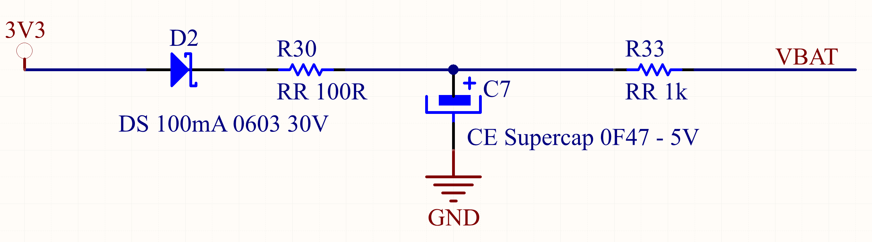
More details about low leakage supercaps can be found in long_lasting_battery_solution document
FUSE2V5
VDDFUSE Powers the fuse box for programming.
VDDFUSE is the only power supply that may be left unpowered during operation. This is possible if and only if the application does not access the Customer Fuse Matrix in Write mode. It is good practice to turn on VDDFUSE only when the Customer Fuse Matrix is accessed in Write mode, and to turn off VDDFUSE otherwise.
VDDFUSE Absolute Maximum Rating is 3.0V. Operating voltage is between 2.25V and 2.75V. A decoupling capacitor of 100 nF is strongly suggested. It must not be left floating.
VDDSDMMC
This pin is used to supply the MCU logic that interfaces the SDMMC peripheral, in order to adjust the logic levels of its I/Os to the external device. I.e.: if the micro SD is powered at 3.3V, the VDDSDMMC can be directly attached to the 3V3 power supply. If, for example, the circuit uses an external eMMC powered at 1.8V, the same power supply, to be realized on the carrier board, must power the VDDSDMMC pin too.
3V3OUT
This is a power out controlled by a mosfet inside the Roadrunner SOM. When the MCU is in shutdown mode, it disables the mosfet cutting out the 3V3 on devices that must be powered off even if the main 3V3 is still on. Maximum current available on this pin is 500mA.
ADVREF
This is the reference voltage for the AD conversion. The conversion is performed on a full range between 0V and the reference voltage pin ADVREF. Analog inputs between these voltages convert to values based on a linear conversion.
External Voltage Reference Input
| Parameter | Min | Typ | Max | Unit |
|---|---|---|---|---|
| ADVREF Input Voltage Range | 2.4 | VDDANA | V | |
| ADVREF Average Current | 600 | μA | ||
| Current Consumption on VDDANA | 600 | μA |
GND
Those are all the pins connected to ground.
As can be seen matching the diagram with the pinout table class='acmetable', they are strategically placed close to the critical signals in order to offer a better shield to crosstalk or other kind of EMI when designing the application board.
Fixed
These pins carry out a specific function and only one each. They cannot be multiplexed with different peripherals.
Most of them are related to the Shutdown Controller (SHDWC) - Details on SAMA5D2 Series datasheet 24. Shutdown Controller (SHDWC)
24.1 Description
The Shutdown Controller (SHDWC) controls the power supplies VDDIO and VDDCORE and the wakeup detection on debounced input lines.
24.2 Embedded Characteristics
- Shutdown Logic
- Software Assertion of the Shutdown Output Pin (SHDN )
- Programmable deassertion from the PIOBU, WKUP Input Pins
- Wakeup Logic
- Programmable Assertion from the PIOBU, WKUP Input Pins, and Internal Wakeup Event from RTC, RXLP, ACC, Security Module
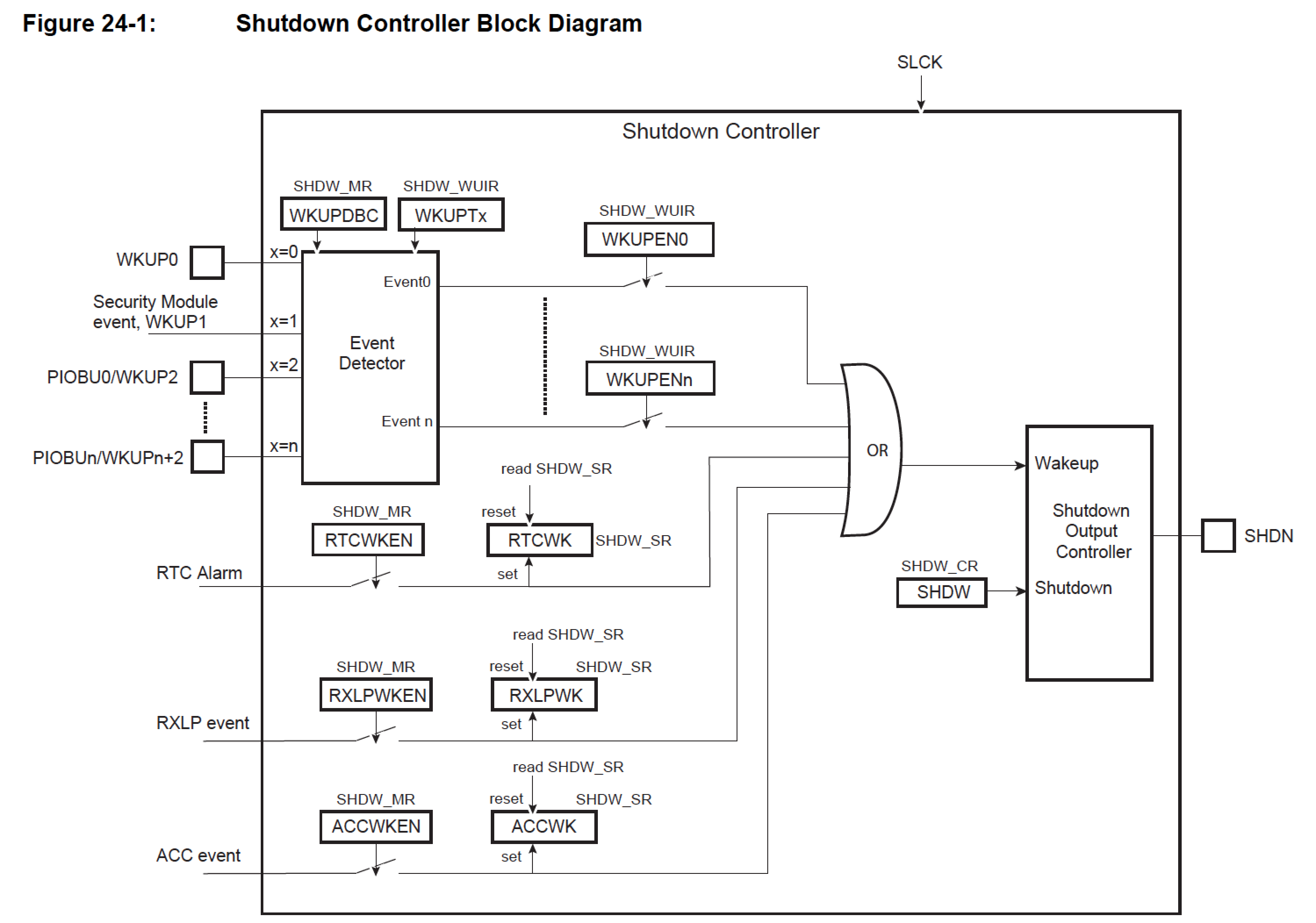
| Name | Description | Type |
|---|---|---|
| WKUP0 | Wakeup inputs | Input |
| PIOBU 0-7 | Wakeup inputs, WKUP(2-9) | Input (2-7 only are exposed on J1 connector) |
| SHDN | Shutdown output | Output |
| BU_RxD | RXLP Receive Data | Input |
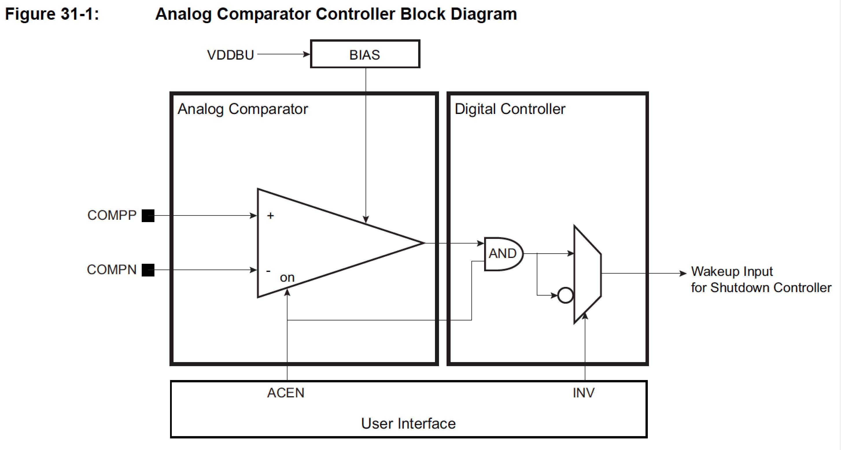
| COMPP, COMPN | External analog data input | Input |
BU_RXD
This is the input pin for RXLP. The RXLP features an RS232 receive-only circuitry able to decode and compare data and parity while the system is in Backup mode. If a matching comparison occurs, the RXLP instructs the system to wake up (if enabled).
30. Low Power Asynchronous Receiver (RXLP)
30.1 Description
The Low Power Asynchronous Receiver (RXLP) is a low-power UART with a slow clock. It works only in Receive mode. It features a Receive Data (RXD) pin that can be used to wake up the system. The wakeup occurs only on data matching—expected data can be a single value, two values, or a range of values. The RXLP operates on a slow clock domain to reduce power consumption.
COMPP-COMPN
Pins reserved to Analog Comparator Controller (ACC). The Analog Comparator Controller (ACC) controls the analog comparator in order to provide an additional source of wakeup when the system wakes up from Wait mode.
BOOT_OFF
In this version of Roadrunner the at91bootstrap is loaded from the on board QSPI Flash memory. The at91bootstrap loads the kernel from QSPI Flash to RAM and then refers to the microSD card for the file system. Grounding BOOT_OFF disables the boot from internal QSPI.
The standard QSPI Flash memory has a capacity of 16MBytes, enough to start the sequence abovementioned. On request it can be installed in a size of up to 256 MByte, enough to accommodate a full Linux OS for a very small system, 100 times more reliable then a microSD card based one.
JTAGSEL
If tied to 3V3 it enables JTAG Boundary Scan. There is an internal pull-down resistor to GNDBU (15 kΩ). In harsh environments it is strongly recommended to tie this pin to GND if not used or to add an external low-value resistor (such as 1 kΩ).
Shared
The pins belonging to this group can be dynamically multiplexed with up to 8 different peripherals.
A table class='acmetable' with a quick guide to the peripherals which can be shared on each pin is available here. For a detailed description of each peripheral, please look at SAMA5D2 Series datasheet
Design suggestions and examples for some common peripherals, are available on How to design the carrier circuitries for our Linux modules section of the Documentation page
Reserved at BOOT
The pins:
- PA22 SCK
- PA23 CS
- PA24 IO0
- PA25 IO1
- PA26 IO2
- PA27 IO3
are connected to the QSPI Flash memory device internally involved in the boot sequence.
After the BOOT passes the control to the system on microSD card, they can be shared with other peripherals if needed. The SCK line on PA22 can also be directly tied to the microSD clock. Of course the correct working of those lines depends on what it's connected to at startup. While accessing the QSPI Flash they work at 133 MHz, also a long track can introduce enough capacity to disturb signal integrity.
Related links
Related products

- CPU Microchip SAMA5D27
- Cortex A5 @ 500 MHz
- Low power consumption:
Suspend to RAM mode 10mW
Full speed: 396mW - Debian, Buildroot and Yocto Linux
- Fully open source drivers
- Low power consumption
- Two USB Host 2.0 ports (one configurable as USB client on the USB-C connector)
- One 10/100 Mbit/s Lan port
- 2 Acme Sensor ports
- Huge set of GPIOS, SPI, I2C and serial lines
- All the circuitries you need to test the RoadRunner SOM
- USB host, USB device, Ethernet port, MicroSD socket
- Test points for power consumption measurements
- All the Roadrunner signals exposed on 2.54mm pitch pins
- On-board supercap for RTC and backup memory circuit
